

Integrated structure for MEMS device and semiconductor device and method of fabricating the same
a technology of integrated structure and semiconductor device, which is applied in the manufacture of microstructural devices, semiconductor devices, electrical apparatus, etc., can solve the problems of lateral damage to the dielectric layer of the cmos device, the dielectric layer adjacent to the sacrificed silicon oxide layer tends to be damaged, and the difficulty in integrating the production of semiconductor devices. to achieve the effect of avoiding the corrosion of the semiconductor devi
- Summary
- Abstract
- Description
- Claims
- Application Information
AI Technical Summary
Benefits of technology
Problems solved by technology
Method used
Image

Examples
Embodiment Construction
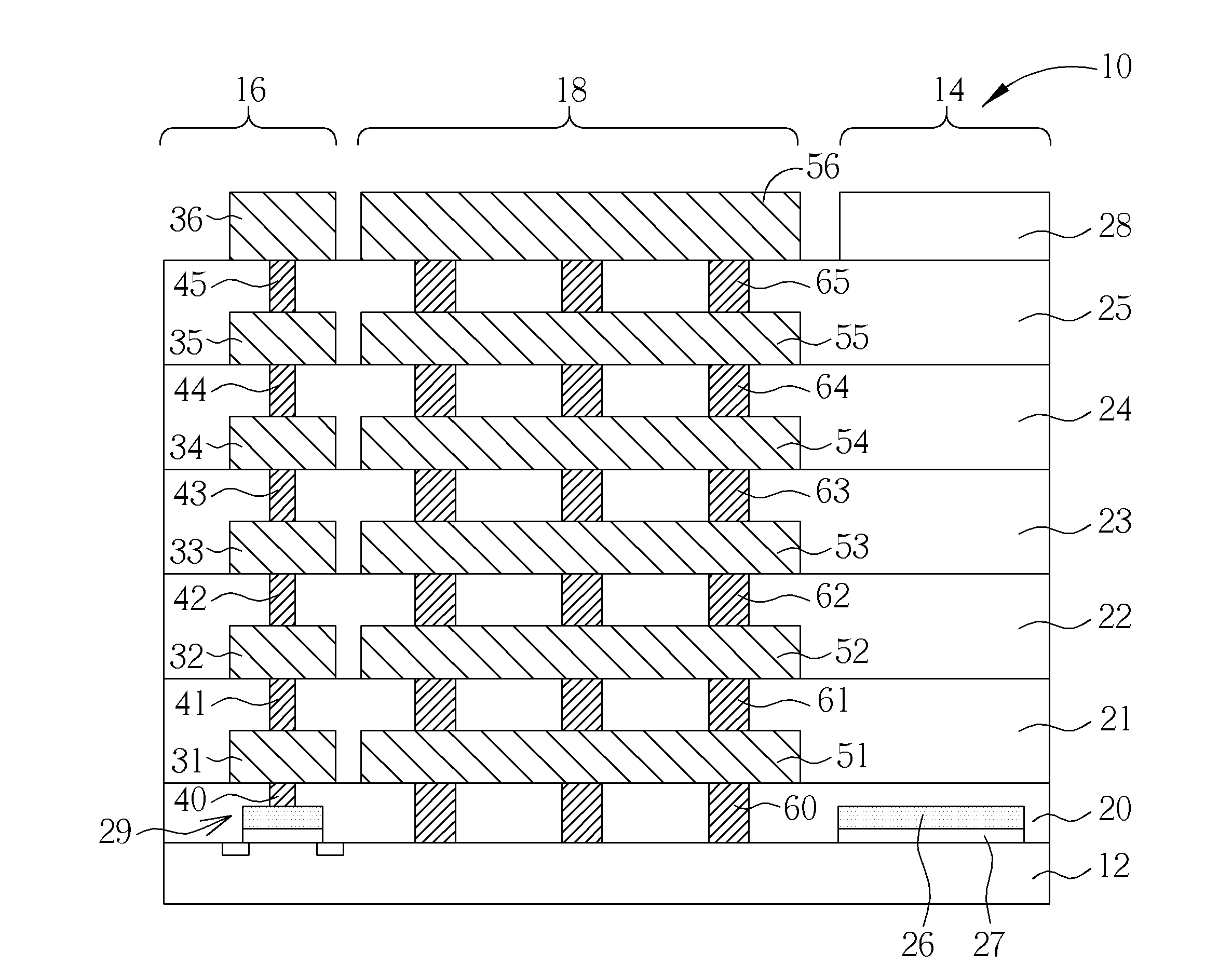
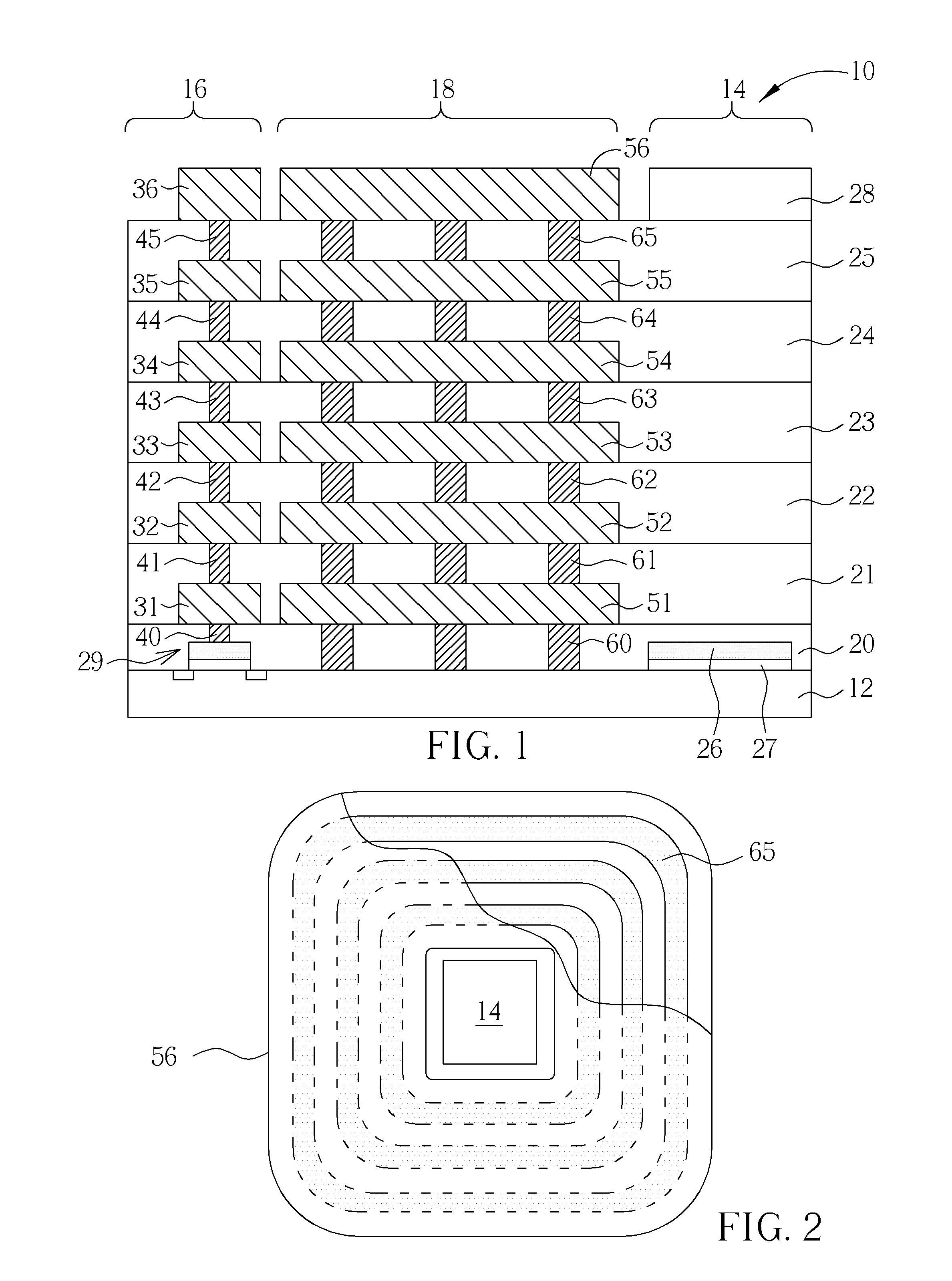
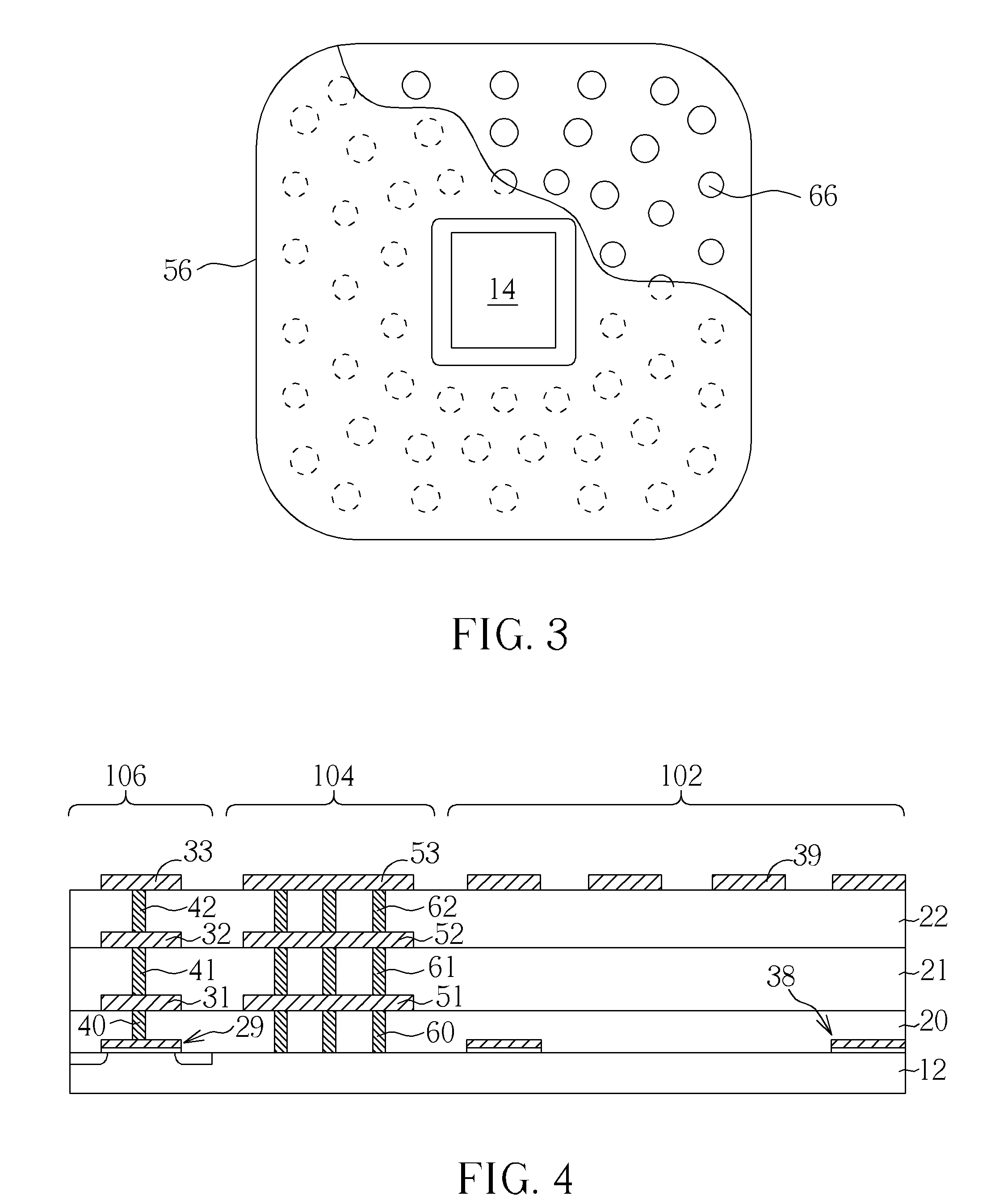
[0018]The integrated structure for a MEMS device and a semiconductor device according to the present invention mainly comprises an etch stopping device formed between the MEMS device and the semiconductor device. In the semiconductor device, a interconnect process is generally performed on the substrate to form a plurality of dielectric layers (or they may be deemed as a whole layer), conductive plugs, and conductive layers. For convenience, the etch stopping device of the present invention may be formed simultaneously with the conductive plugs or the conductive layer using the interconnect process. The semiconductor device may comprise for example, MOS transistors, such as PMOS, NMOS, or CMOS devices.
[0019]In the present invention, the etch stopping device formed between the MEMS device and the semiconductor device to protect the semiconductor device during the release process for making the MEMS device. The etch stopping device may be formed alone or together with the formation of...
PUM
 Abstract
Description
Claims
Application Information