Lead frame and package of semiconductor device

a semiconductor device and lead frame technology, applied in the direction of semiconductor electrostatic transducers, microphone structural associations, transducer casings/cabinets/supports, etc., can solve the problems of difficult production of small-size semiconductor devices, and achieve the effect of large volume, small size and large siz

Inactive Publication Date: 2009-10-01
YAMAHA CORP
View PDF1 Cites 30 Cited by
  • Summary
  • Abstract
  • Description
  • Claims
  • Application Information

AI Technical Summary

Benefits of technology

[0032]As described above, the lead frame having a simple structure is sealed with the mold resin, wherein the interconnection arms are bent downwardly from the main frame to the shield plate. This makes it possible to form the shield plate having a relatively large size by use of the lead frame having a small outline configuration. That is, it is possible to secure a relatively large volume for storing the semiconductor chip within the package having a relatively small size, thus achieving high-density packaging. After the lead frame is sealed with the mold resin, the bent portions of the main frame are subjected to cutting so as to isolate the terminals supported by the support arms independently from the main frame. By attaching the cover having conductivity onto the main frame exposed on the upper end of the peripheral wall, it is possible to reliably shield the internal space from an external magnetic field while reliably insulating the terminals from the cover.

Problems solved by technology

However, it needs a complex bending process in which the interconnection leads are partially bent upwardly so as to expose the intermediate portions thereof on the upper surface of the peripheral wall of the mold resin, then, the distal ends of the interconnection leads are bent downwardly and exposed on the backside of the mold resin.
The semiconductor device of Patent Document 6 suffers from a drawback in which a flat-shaped package base thereof likely allows a bonding agent, which is used for die bonding of the semiconductor chip, to overflow toward the internal ends of the leads.
This makes it difficult to produce small-size semiconductor devices.

Method used


Image

  • Lead frame and package of semiconductor device
  • Lead frame and package of semiconductor device
  • Lead frame and package of semiconductor device

Examples


first embodiment

1. First Embodiment

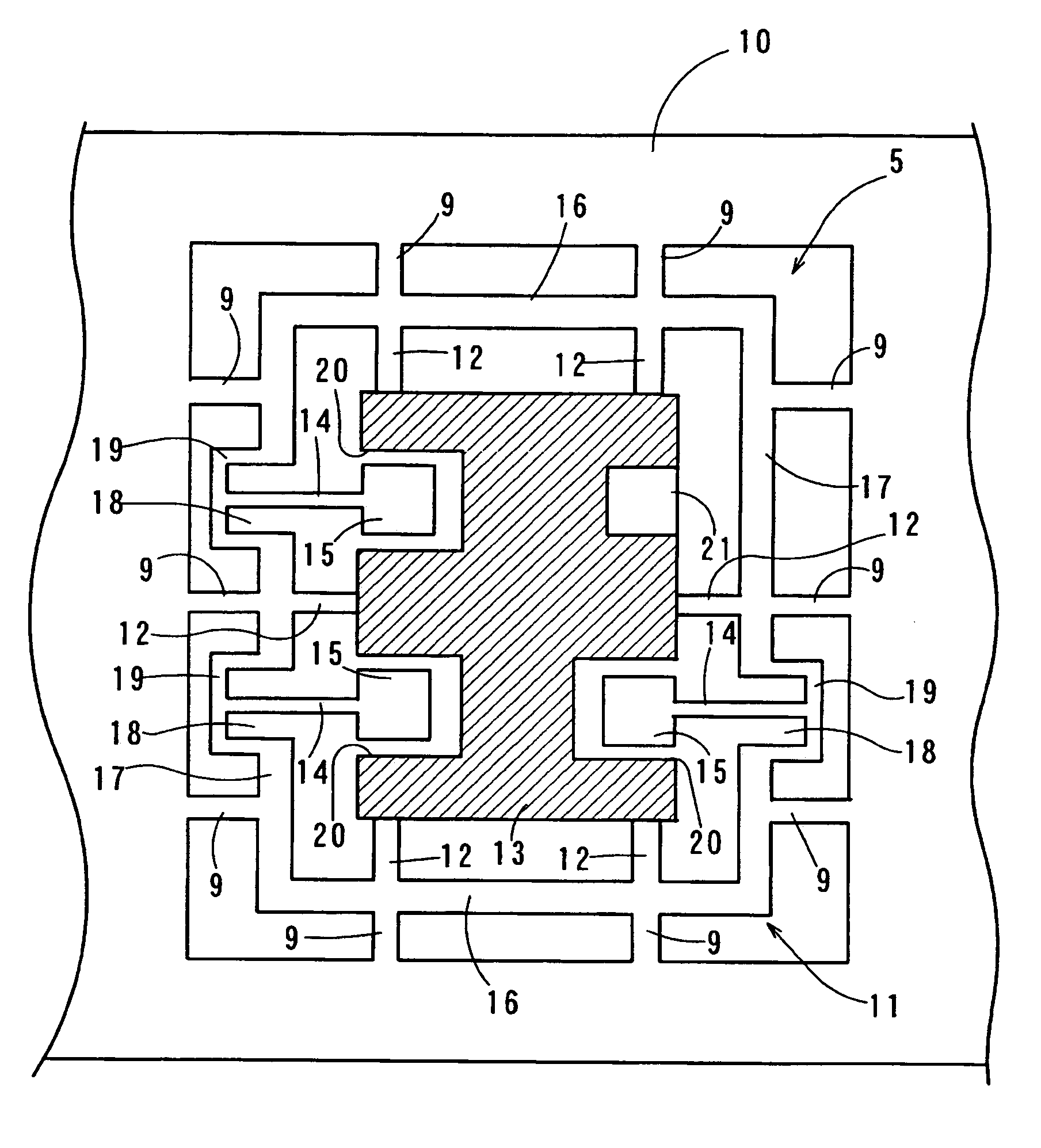
[0098]A semiconductor device 1 according to a first embodiment of the present invention will be described with reference to FIGS. 1 to 8.

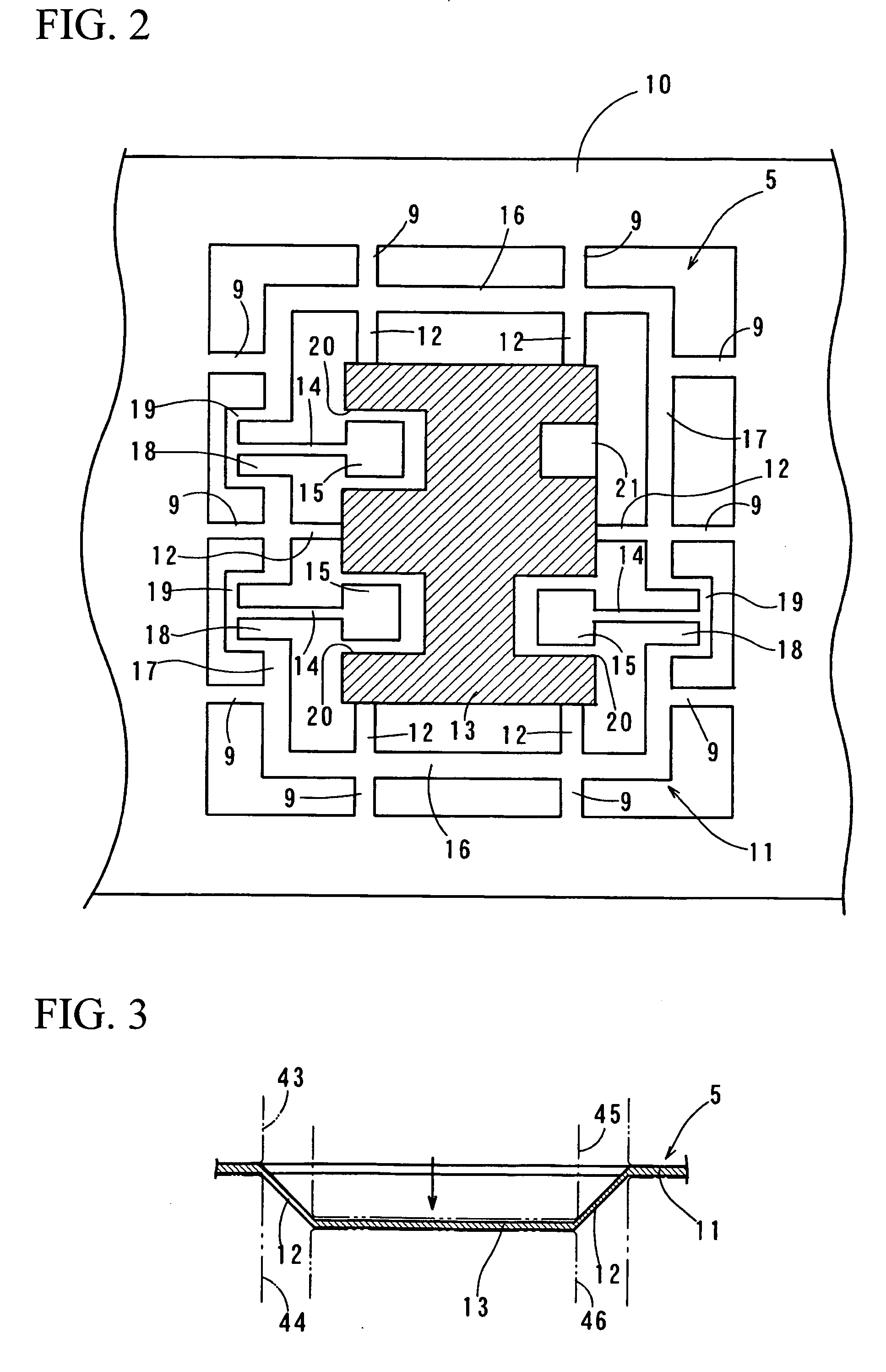
[0099]The semiconductor device 1 is a surface-mount type microphone package, which contains two semiconductor chips, i.e. a microphone chip 2 and a control chip (or a circuit chip) 3 as shown in FIGS. 6 and 7. A package 4 of the semiconductor device 1 is constituted by a package base 7 and a cover 8. The package base 7 is constituted of a lead frame 5 and a box-shaped mold resin 6 which is integrally formed with the lead frame 5. The cover 8 closes the upper section of the package base 7.

[0100]A plurality of lead frames (each corresponding to the lead frame 5) which is aligned in line or in plural lines is collectively formed by way of press working on a sheet-shaped metal plate. In the present specification, the upper / lower direction is referred to as a vertical direction while the left / right direction is referred to as a horizo...

second embodiment

2. Second Embodiment

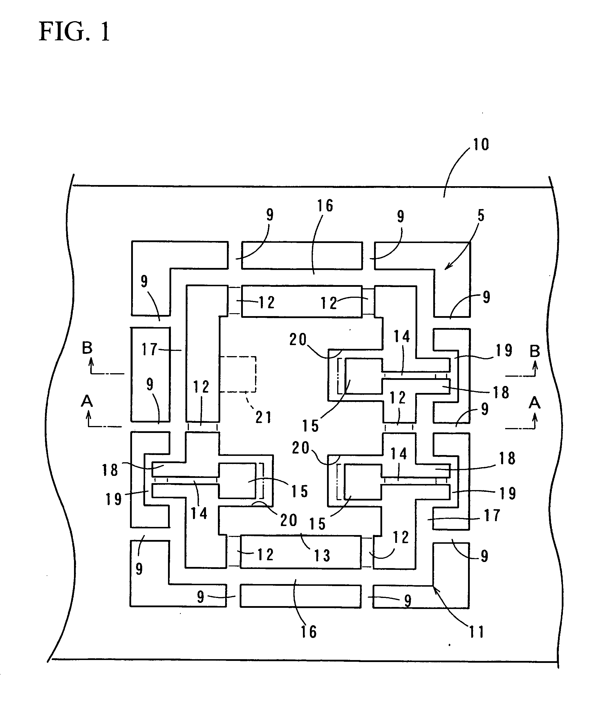
[0125]A semiconductor device according to a second embodiment of the present invention will be described with reference to FIGS. 9 to 12, wherein parts identical to those of the semiconductor device 1 of the first embodiment are designated by the same reference numerals, thus avoiding duplicate descriptions thereof.

[0126]Compared with the lead frame 5 of the first embodiment shown in FIG. 1, a lead frame 61 of the semiconductor device of the second embodiment is characterized in that slits 62 are additionally formed to partially cut into the shield plate 13 so as to further extend the interconnection arms 12 derived from the center positions of the longitudinal frames 17. That is, the distal ends of the interconnection arms 12 are disposed at the recessed positions on the longitudinal sides of the shield plate 13. When the shield plate 13 is subjected to pressing and is depressed in position compared to the main frame 11, the interconnection arms 12 are each bent...

third embodiment

3. Third Embodiment

[0130]A semiconductor device according to a third embodiment of the present invention will be described with reference to FIG. 16, wherein it is characterized by modifying the structure for supporting the terminals 15 in a lead frame 85, compared to the lead frames 5 and 61 of the first and second embodiments. In the first and second embodiments, the terminals 15 are disposed independently of the shield plate 13 and are cantilevered and supported by the support arms 14 derived from the main frame 11. The lead frame 85 is designed without using the support arms 14 such that the terminals 15 positioned inside of the cutouts 20 of the shield plate 13 are interconnected to the shield plate 13 via a plurality of bridges 86. After completion of resin molding, the bridges 86 are subjected to laser cutting so as to separate the terminals 15 from the shield plate 13. In the first and second embodiments in which the support arms 14 are bent and deformed so as to move the te...


PUM


Abstract

A lead frame including a shield plate, a main frame, interconnection arms, support arms, and terminals is sealed with a resin mold including a base portion for embedding the shield plate and a peripheral wall for embedding the interconnection arms and support arms, thus forming a package base. The interconnection arms and support arms are subjected to bending so as to depress the shield plate in position compared with the main frame. At least one semiconductor chip (e.g. a microphone chip) is mounted on the base portion just above the shield plate. A cover having conductivity is attached onto the main frame exposed on the upper end of the peripheral wall, thus completely producing a semiconductor device encapsulated in a package. A sound hole is formed in the cover or the package base so as to allow the internal space of the package to communicate with the external space.

Description

BACKGROUND OF THE INVENTION[0001]1. Field of the Invention[0002]The present invention relates to lead frames and packages for use in semiconductor devices, wherein semiconductor chips are mounted on package bases including lead frames sealed with mold resins.[0003]The present application claims priority on Japanese Patent Application No. 2008-90475, Japanese Patent Application No. 2008-155370, and Japanese Patent Application No. 2008-248228, the contents of which are incorporated herein by reference.[0004]2. Description of the Related Art[0005]Conventionally, semiconductor devices such as silicon microphones and pressure sensors are designed such that semiconductor chips such as microphone chips are encapsulated in hollow packages of a pre-mold type in which lead frames are sealed with mold resins in advance. Various types of conventionally-known semiconductor devices encapsulated in pre-mold type packages have been developed and disclosed in various documents such as Patent Documen...

Claims


Application Information

Patent Timeline
Patent Type & Authority Applications(United States)
IPC IPC(8): H01L23/495H01L21/00
CPCH01L2224/48245H04R1/04H04R1/06H04R19/005H01L2924/01019H01L2924/01087H01L2224/48247H01L2924/1461H01L2924/3025H01L2924/00H01L2224/05554H01L2224/48091H01L2224/48137H01L2224/49171H01L2224/49175H01L2224/48465H01L2224/73265H01L2924/16151H01L2924/16195H01L2924/00014H01L23/48H01L23/28
Inventor SHIRASAKA, KENICHI
Owner YAMAHA CORP
Why Eureka
Try Eureka