Semiconductor Device and Method for Manufacturing Semiconductor Device

a semiconductor and semiconductor technology, applied in the direction of semiconductor devices, semiconductor/solid-state device details, electrical apparatus, etc., can solve the problems of inhibiting a decrease in joint reliability, reducing the bending of the substrate, and insufficient coupling between the substrate and the electrode, so as to improve joint reliability, reduce elastic modulus, and enhance the effect of adhesiveness

Inactive Publication Date: 2009-10-01
SUMITOMO BAKELITE CO LTD
View PDF7 Cites 154 Cited by
  • Summary
  • Abstract
  • Description
  • Claims
  • Application Information

AI Technical Summary

Benefits of technology

[0038]According to this configuration, through solder, the conductor interconnect layer of the first resin substrate is coupled to the conductor interconnect layer of the resin spacer, and the conductor interconnect layer of the second resin substrate is coupled to the conductor interconnect layer of the resin spacer. Therefore, metallic junctions can be formed between solder and the conductor interconnect layer of the first resin substrate, between solder and the conductor interconnect layer of the resin spacer and between solder and the conductor interconnect layer of the second resin substrate. This allows providing the semiconductor device with an improved joint reliability.
[0039]In addition, it is preferable that a first resin layer of the first adhesive member and a second resin layer of the second adhesive member contain an epoxy resin and an acrylic rubber. The first resin layer and the second resin layer are composed of materials containing an acrylic rubber, so that a reduced elastic modulus is achieved and an enhanced adhesiveness to the first resin substrate, the resin spacer and the second resin substrate is achieved for the first adhesive member and the second adhesive member. Further, the first resin layer and the second resin layer are composed of materials containing epoxy resin, so that an enhanced heat resistance and an enhanced moisture resistance are achieved for the first adhesive member and the second adhesive member.

Problems solved by technology

Thus, reliability in the coupling between the substrate and the electrode may be insufficient.
The resin spacer is provided between the resin substrates, in place of providing the bump electrode, so that a difference in the coefficient of thermal expansion between the upper and lower substrates and the spacer can be zero or reduced, leading to reducing a stress of a vertical connection with an electric conduction, and leading to a reduction in the bending of the substrate, thereby inhibiting a decrease in the joint reliability.

Method used


Image

  • Semiconductor Device and Method for Manufacturing Semiconductor Device
  • Semiconductor Device and Method for Manufacturing Semiconductor Device
  • Semiconductor Device and Method for Manufacturing Semiconductor Device

Examples


first embodiment

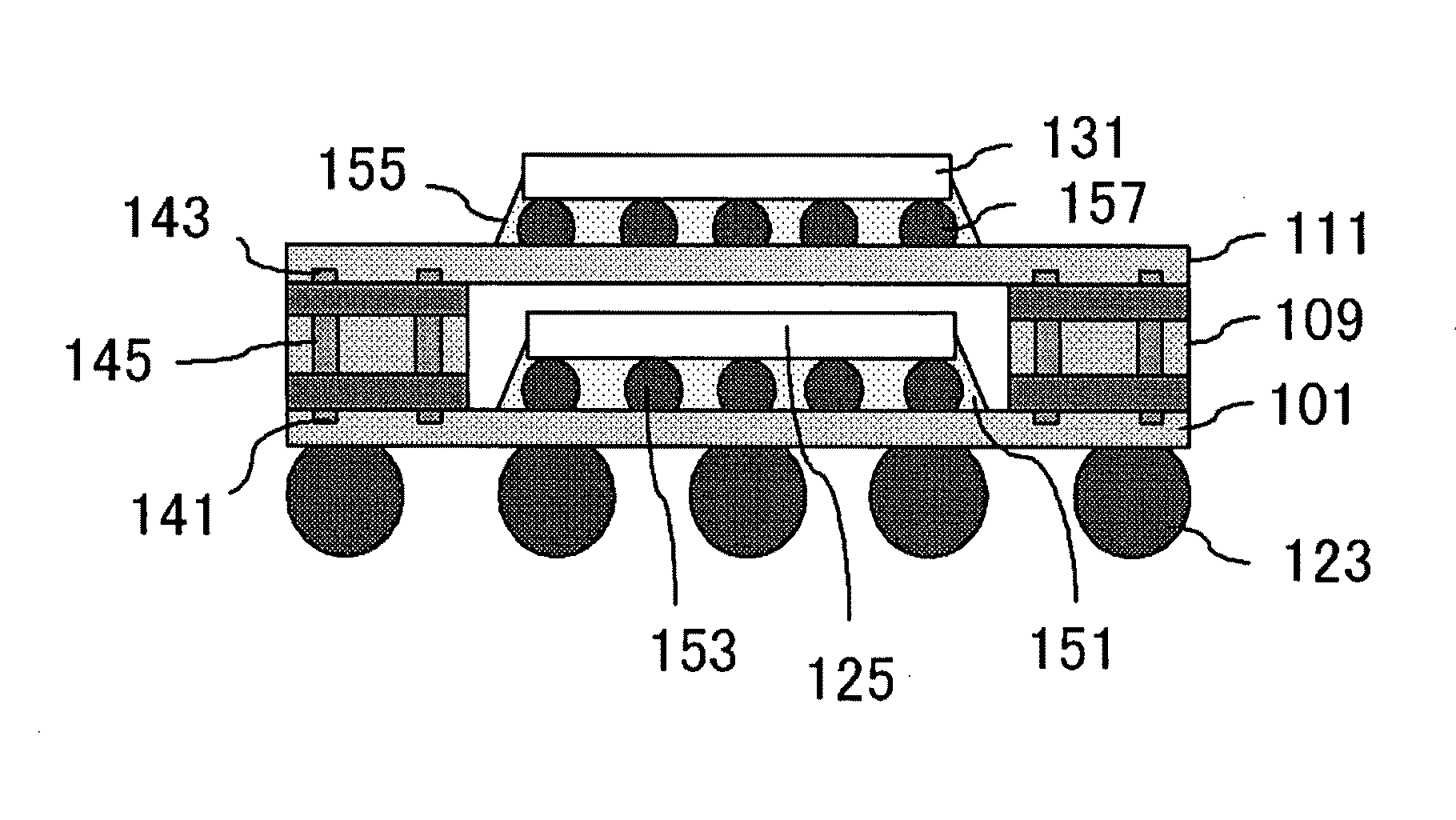
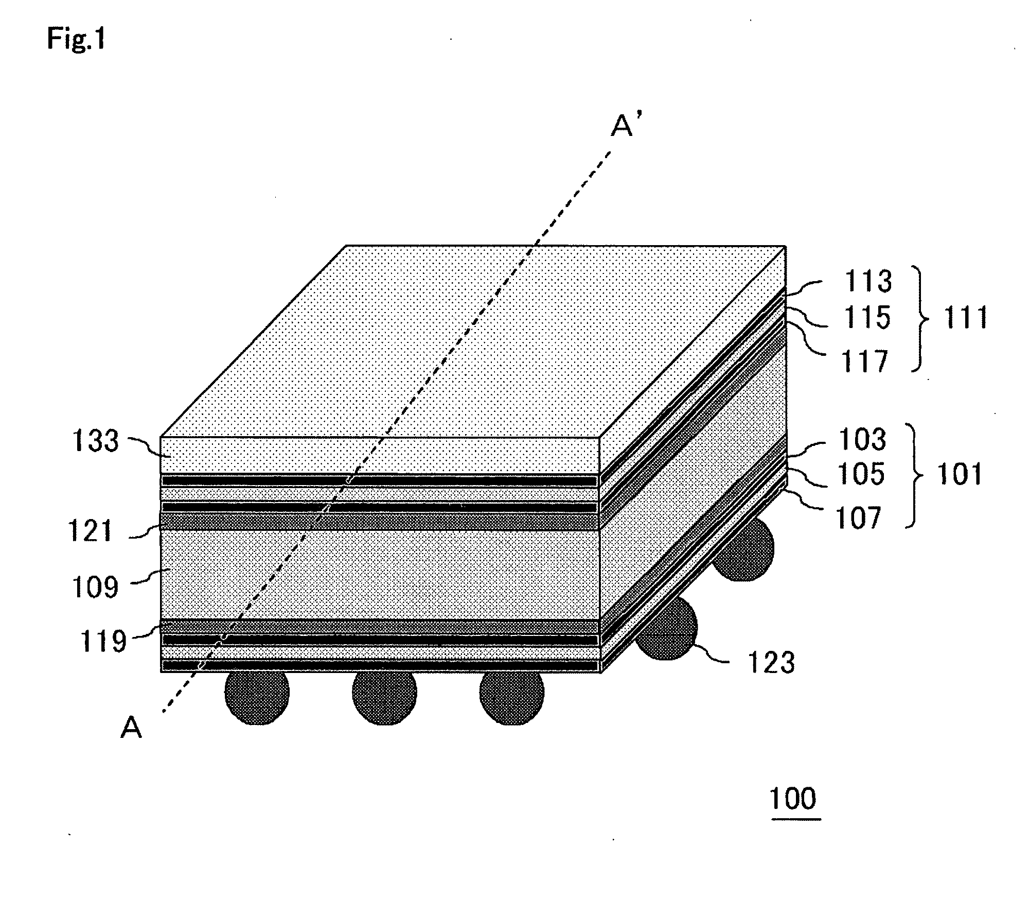
[0088]FIG. 1 is a perspective view, illustrating a configuration of a semiconductor device of the present embodiment. FIG. 2 is a cross-sectional view of FIG. 1 along line A-A′. In a semiconductor device 100 shown in FIG. 1 and FIG. 2, a first resin substrate 101, an adhesive layer 119, a resin spacer (resin base material 109), an adhesive layer 121 and a second resin substrate 111 are stacked in this sequence from underneath.

[0089]This semiconductor device 100 has a POP structure, and a first semiconductor chip 125 is mounted on a surface of the first resin substrate 101, and a second semiconductor chip 131 is mounted on a surface of the second resin substrate 111.

[0090]The first semiconductor chip 125 and the second semiconductor chip 131 are semiconductor chips, having certain elements such as transistor and the like formed on a device-forming surface of a semiconductor substrate such as silicon substrate and the like, respectively. The first semiconductor chip 125 may be configu...

second embodiment

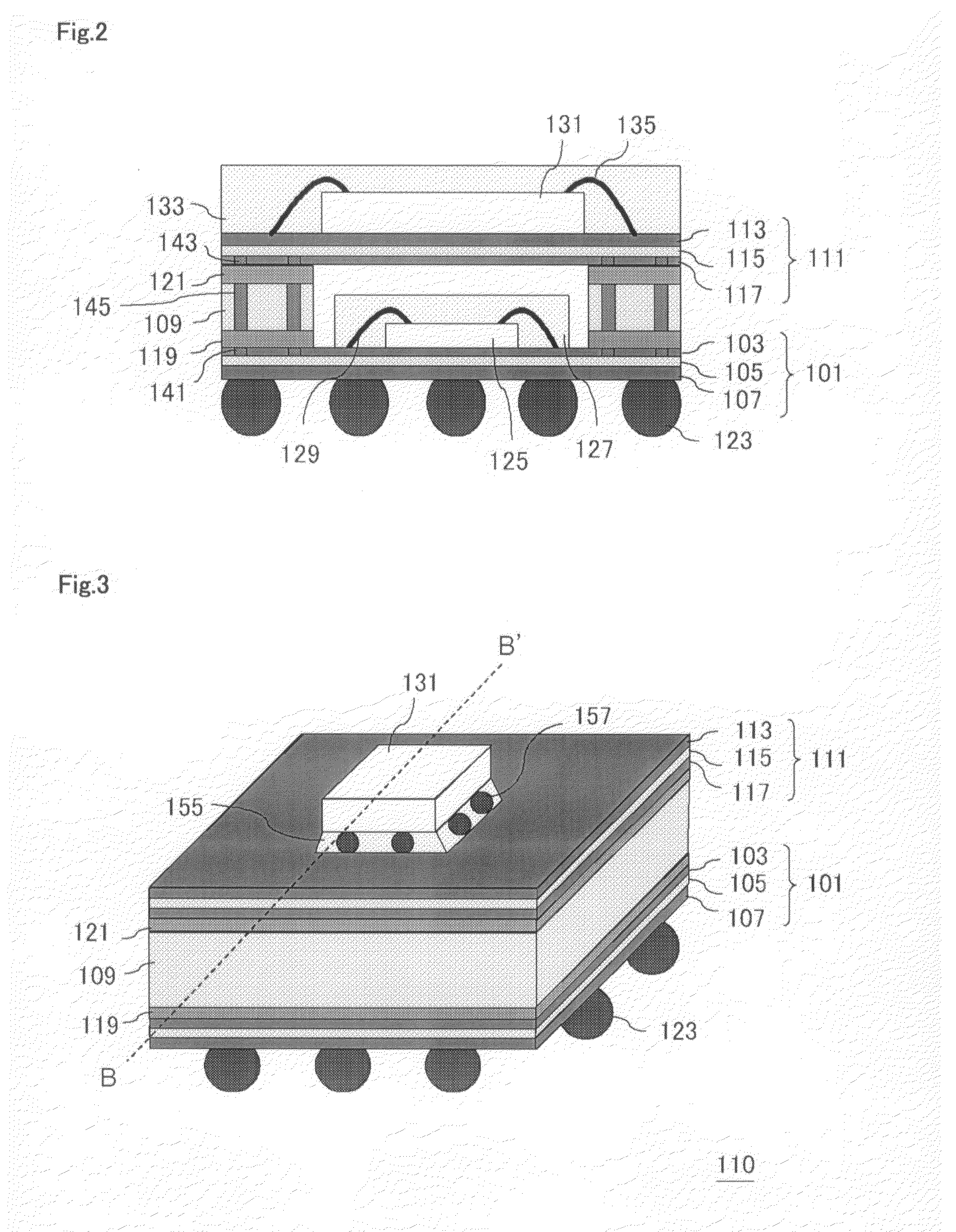
[0129]While the configuration having the semiconductor chip wire-bonded onto the resin substrate has been illustrated in relation to the semiconductor device described in first embodiment, the semiconductor chip may be flip-connected to the resin substrate via the bump electrode. The present embodiment will describe such configuration.

[0130]FIG. 3 is a perspective view, illustrating a configuration of a semiconductor device in the present embodiment. FIG. 4 is a cross-sectional view along line B-B′ of FIG. 3.

The fundamental configurations of semiconductor devices 110 shown in FIG. 3 and FIG. 4 are similar to that of the semiconductor device 100 (FIG. 1, FIG. 2), except that the method of mounting the semiconductor chip onto the resin substrate is different therefrom.

[0131]In the semiconductor device 110, an electrode (not shown) provided on the element mounting surface of the first semiconductor chip 125 is joined to the electrode (not shown) provided on the built-up 103 of the firs...

third embodiment

[0145]An embodiment of the present invention will be described as follows, on the basis of the annexed figures. First of all, an outline of a semiconductor device 1 according to the present embodiment will be described in reference to FIG. 12 to FIG. 17. The semiconductor device 1 includes, as shown in FIG. 12 and FIG. 13, a first resin substrate 3 on which a first semiconductor chip 2 is mounted, a second resin substrate 5 on which a second semiconductor chip 4 is mounted, and a resin spacer 6, which is in contact with a front surface of the first resin substrate 3 and a back surface of the second resin substrate 5, and provides an electrical juncture between the first resin substrate 3 and the second resin substrate 5. FIG. 13 is a cross-sectional view along II-II direction of FIG. 12. The resin spacer 6 is disposed in a circumference of the first semiconductor chip 2 on the front surface of the first resin substrate 3, and, on the front surface of the first resin substrate 3, the...


PUM


Abstract

A semiconductor device (100) comprises a first resin substrate (101) on which a first semiconductor chip (125) is mounted a surface thereof; a second resin substrate (111) on which a second semiconductor chip (131) is mounted on a surface thereof; and a resin base material (109), joined to a front surface of the first resin substrate (101) and to a back surface of the second resin substrate (111), so that these surfaces are electrically connected. The resin base material (109) is disposed in a circumference of the first resin substrate (101) in the surface of the first resin substrate (101). Further, the first semiconductor chip (125) is disposed in a space section provided among the first resin substrate (101), the second resin substrate (111) and the resin base material (109) in the surface of the first resin substrate (101).

Description

BACKGROUND[0001]1. Technical Field[0002]The present invention relates to a semiconductor device, and particularly relates to a semiconductor device having a plurality of stacked semiconductor chips and a method for manufacturing a semiconductor device.[0003]2. Background Art[0004]In recent years, lighter, more compact and more sophisticated semiconductor devices are generally required in the industry, and a dense integration of electronic components and a dense installation of electronic components are progressed. Semiconductor packages employed for these electronic equipments are miniaturized and have multiple pins, and further, substrates for packaging electronic components including semiconductor packages are also miniaturized.[0005]Typical semiconductor packages that achieves a high-density package include a stack structure, in which a plurality of semiconductor chips are stacked on an interconnect substrate. When a combination of a larger semiconductor chip and a smaller semico...

Claims


Application Information

Patent Timeline
Patent Type & Authority Applications(United States)
IPC IPC(8): H01L23/498H01L23/00H01L23/28H01L21/50H01L21/56
CPCH01L23/16H01L2924/07802H01L23/562H01L25/0657H01L25/105H01L25/18H01L2224/16225H01L2224/48091H01L2224/48227H01L2224/73204H01L2225/0651H01L2225/06517H01L2225/0652H01L2225/06541H01L2225/06551H01L2225/06572H01L2225/06582H01L2225/06586H01L2924/01012H01L2924/0102H01L2924/01046H01L2924/01078H01L2924/01079H01L2924/09701H01L2924/15311H01L2924/15331H01L23/3128H01L2924/07811H01L2924/12041H01L2225/107H01L24/48H01L2924/01019H01L2924/01087H01L2224/32225H01L2924/3511H01L2224/73265H01L2225/1023H01L2225/1058H01L2924/00014H01L2924/00H01L2924/00012H01L2924/12042H01L24/73H01L2924/14H01L2924/181H01L2224/45099H01L2224/45015H01L2924/207H01L25/11
Inventor SUGINO, MITSUOKATSURAYAMA, SATORUYAMASHIRO, TOMOEMIYAMOTO, TETSUYAYAMASHITA, HIROYUKI
Owner SUMITOMO BAKELITE CO LTD
Why Eureka
Try Eureka