Structure and method for elimination of process-related defects in poly/metal plate capacitors

a poly/metal plate capacitor and process-related technology, applied in the direction of capacitors, semiconductor devices, electrical equipment, etc., can solve the problems of cone defects, inability to develop silicon etchants, etc., and achieve the effect of avoiding the damaging effect of silicon cone defects

Inactive Publication Date: 2009-10-08
TEXAS INSTR INC
View PDF7 Cites 15 Cited by
  • Summary
  • Abstract
  • Description
  • Claims
  • Application Information

AI Technical Summary

Benefits of technology

[0011]It is an object of the invention to provide an integrated circuit process and an integrated circuit structure which avoid damaging effects of silicon cone defects.

Problems solved by technology

So far, it has not been possible to develop a silicon etchant which does not result in creation of cone defects.
An electrical short circuit caused by silicon cone defect 22 in FIG. 1 usually has very low impedance, and therefore can create “massive” failures such as causing sufficiently high current to flow through metal traces and through poly layer 5 into epi layer 2 so as to vaporize metal traces in the integrated circuit chip.

Method used


Image

  • Structure and method for elimination of process-related defects in poly/metal plate capacitors
  • Structure and method for elimination of process-related defects in poly/metal plate capacitors
  • Structure and method for elimination of process-related defects in poly/metal plate capacitors

Examples


Embodiment Construction

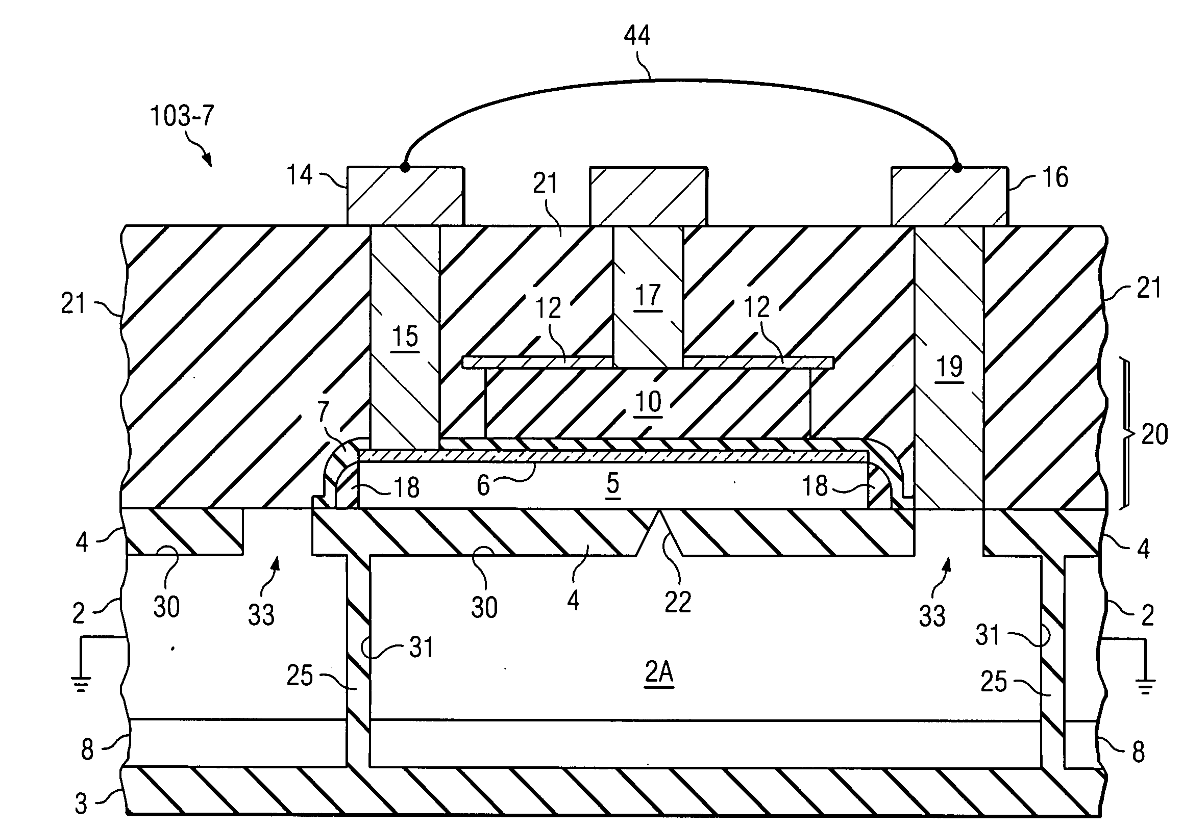
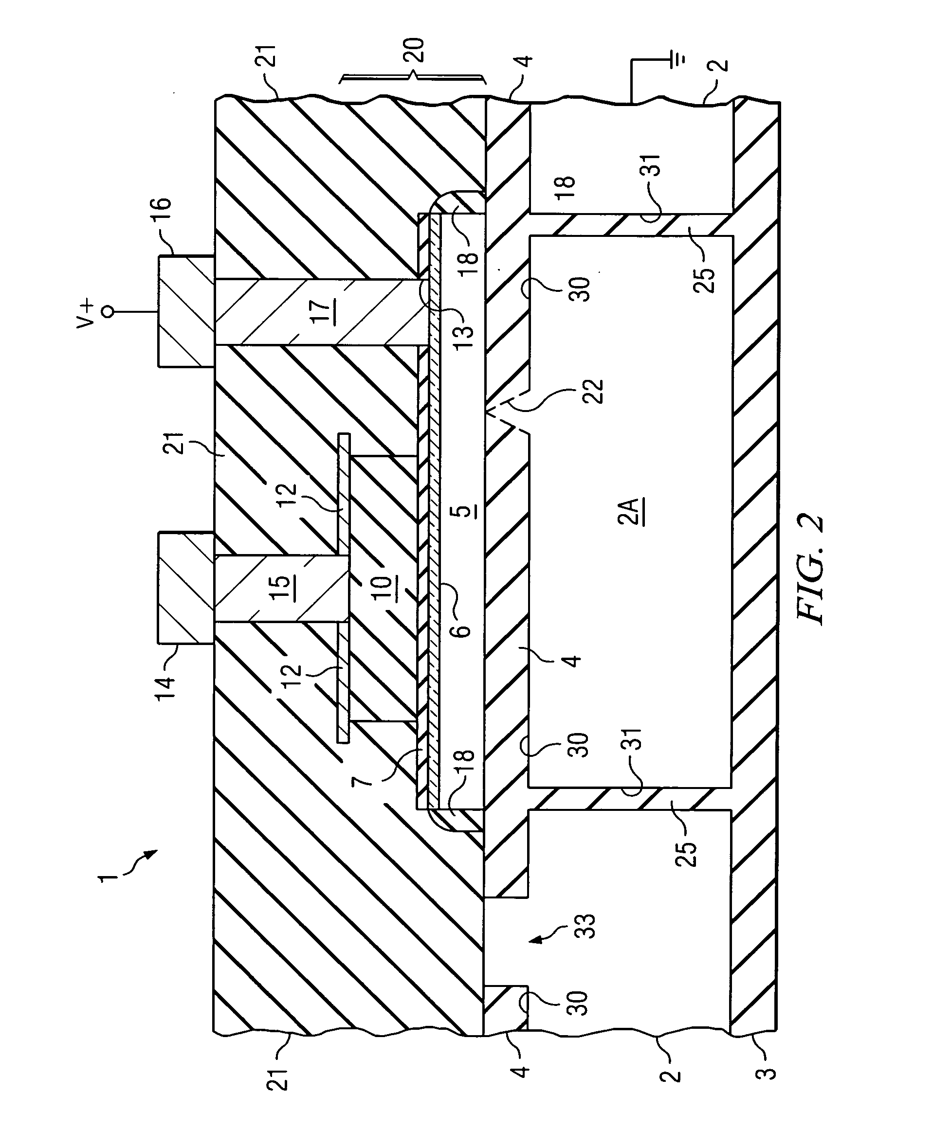
[0027]Referring to FIG. 2, integrated circuit structure 100 includes the same poly / metal plate capacitor 20 shown in Prior Art FIG. 1, which is formed using a shallow trench isolation (STI) process. Integrated circuit structure 100 in FIG. 2 is also formed using a shallow trench isolation process, and includes a bottom oxide layer 3 which is formed on the bottom surface of single crystal silicon wafer substrate 8. As in Prior Art FIG. 1, bottom oxide layer 3 is supported by a silicon support wafer (not shown) such as support wafer 9 in FIG. 1. A N-type epi layer 2 is formed on the upper surface of silicon substrate 8, as in Prior Art FIG. 1. Shallow trench oxide layer 4, which can be formed of SiO2, is formed on epi layer 2. The shallow trenches 30, in which shallow trench oxide layer 4 is formed, can be approximately 500 nanometers deep. Shallow trench oxide layer 4 preferably is of the same thickness as the shallow trench depth. P-type poly layer 5 is formed on shallow trench oxid...


PUM


Abstract

An integrated circuit includes silicon layer (2) supported by a bottom oxide layer (3), a shallow trench oxide (4) in the shallow trench (30), and a polycrystalline silicon layer (5) on the shallow trench oxide. A deep trench oxide (25) extending from the shallow trench oxide to the bottom oxide layer electrically isolates a section (2A) of the silicon layer to prevent a silicon cone defect (22) on the silicon layer (2) from causing short-circuiting of the polycrystalline silicon layer (5) to a non-isolated section of the silicon layer. The polycrystalline silicon layer (5) can form a bottom plate of a poly/metal capacitor (20) and can also form a poly interconnect conductor (5A).

Description

CROSS REFERENCE TO RELATED APPLICATION[0001]This application claims the benefit of prior filed co-pending U.S. provisional application Ser. No. 61 / 123,325 entitled “STRUCTURE AND METHOD FOR ELIMINATION OF PROCESS-RELATED DEFECTS IN POLY / METAL PLATE CAPACITORS”, filed Apr. 8, 2008 by Walter B. Meinel, Henry Surtihadi, Phillipp Steinmann, and David J. Hannaman, and incorporated herein by reference.BACKGROUND OF THE INVENTION[0002]The present invention relates generally to methods and integrated circuit structures for avoiding the damaging effects of silicon cone defects.[0003]Referring to FIG. 1, a known integrated circuit structure 1 includes a doped polycrystalline silicon (poly) / titanium nitride (TiN) plate capacitor, referred to herein as a poly / metal plate capacitor. The integrated circuit structure 1 is formed using a shallow trench isolation (STI) process. Integrated circuit structure 1 includes a bottom oxide layer 3 which is formed on the bottom surface of a single crystal si...

Claims


Application Information

Patent Timeline
Patent Type & Authority Applications(United States)
IPC IPC(8): H01L29/94H01L21/02
CPCH01L21/84H01L28/60H01L27/1203H01L21/76232H01L21/76283
Inventor MEINEL, WALTER B.SURTIHADI, HENRYSTEINMANN, PHILIPPHANNAMAN, DAVID J.
Owner TEXAS INSTR INC
Why Eureka
Try Eureka