Method of heat-treating semiconductor

a heat-treating and semiconductor technology, applied in the direction of semiconductor devices, electrical equipment, basic electric elements, etc., can solve the problems of high manufacturing cost, long manufacturing time, large energy consumption, etc., and achieve the effect of stable heat-treating, short processing time and low energy consumption

Inactive Publication Date: 2009-10-08
HIGHTEC SYST CORP
View PDF4 Cites 19 Cited by
  • Summary
  • Abstract
  • Description
  • Claims
  • Application Information

AI Technical Summary

Benefits of technology

[0028]By using the heat-treating method of the present invention, stable heat-treating with low energy consumption and processing in a short period of time can be realized.
[0029]It is needless to say that with this heat-treating, phase-shifti

Problems solved by technology

However, in the technique disclosed in Patent Document 1, etc., there are problems that heating at a high temperature for a long period of time is necessary, energy consumption is large, the manufacture time is long, and the manufacturing cost is high.
On the other hand, in the method of using a semiconductor laser light as in the technique described in Patent Document 2, there is a problem that energy los

Method used


Image

  • Method of heat-treating semiconductor
  • Method of heat-treating semiconductor
  • Method of heat-treating semiconductor

Examples


Embodiment Construction

[0041]Below, with respect to an embodiment of the present invention, description will be made referring to drawings. However, the present invention is not limited to this.

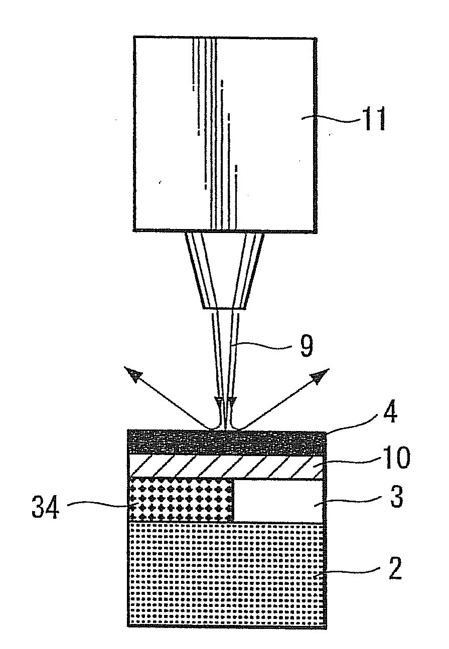
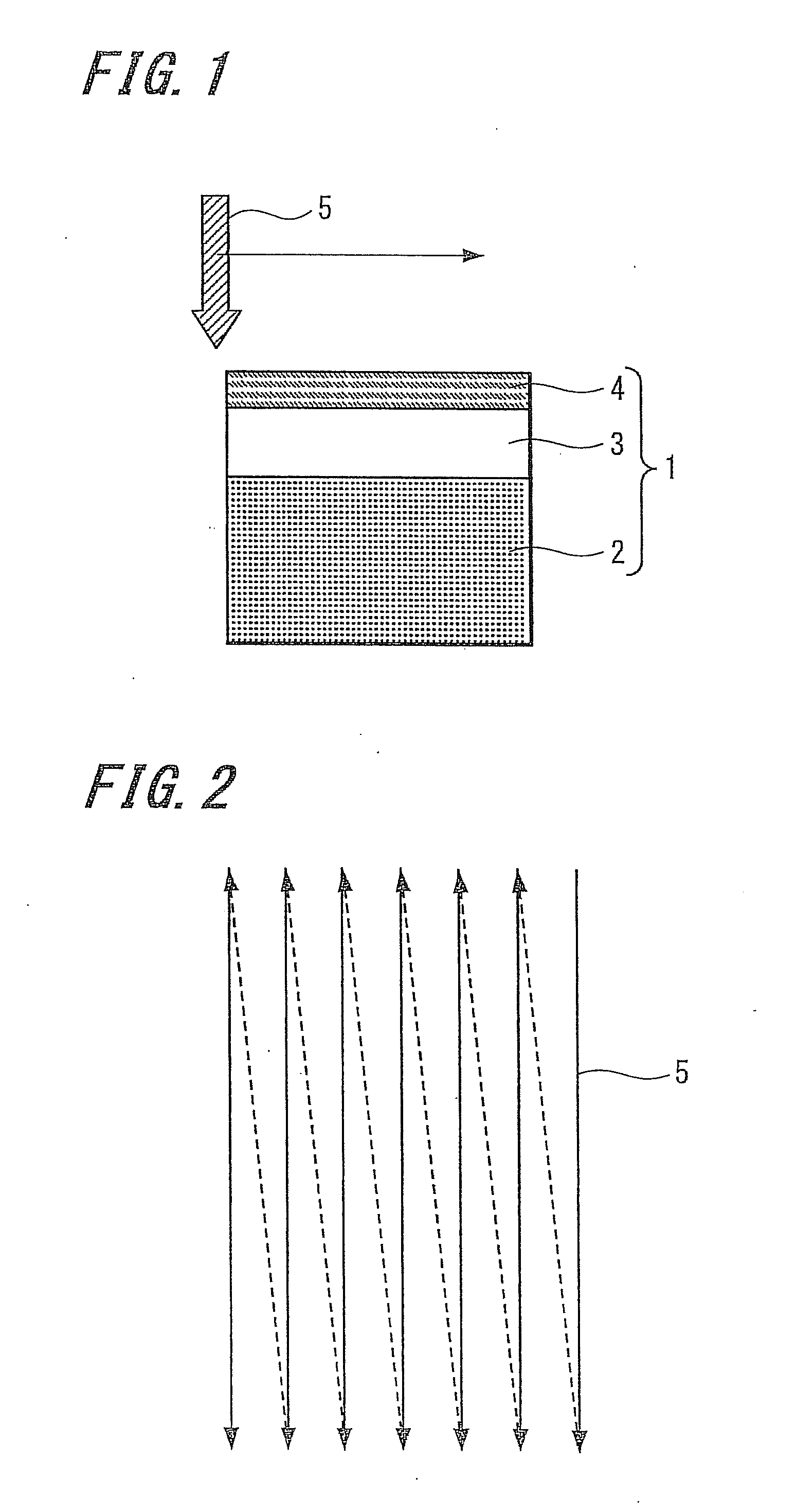
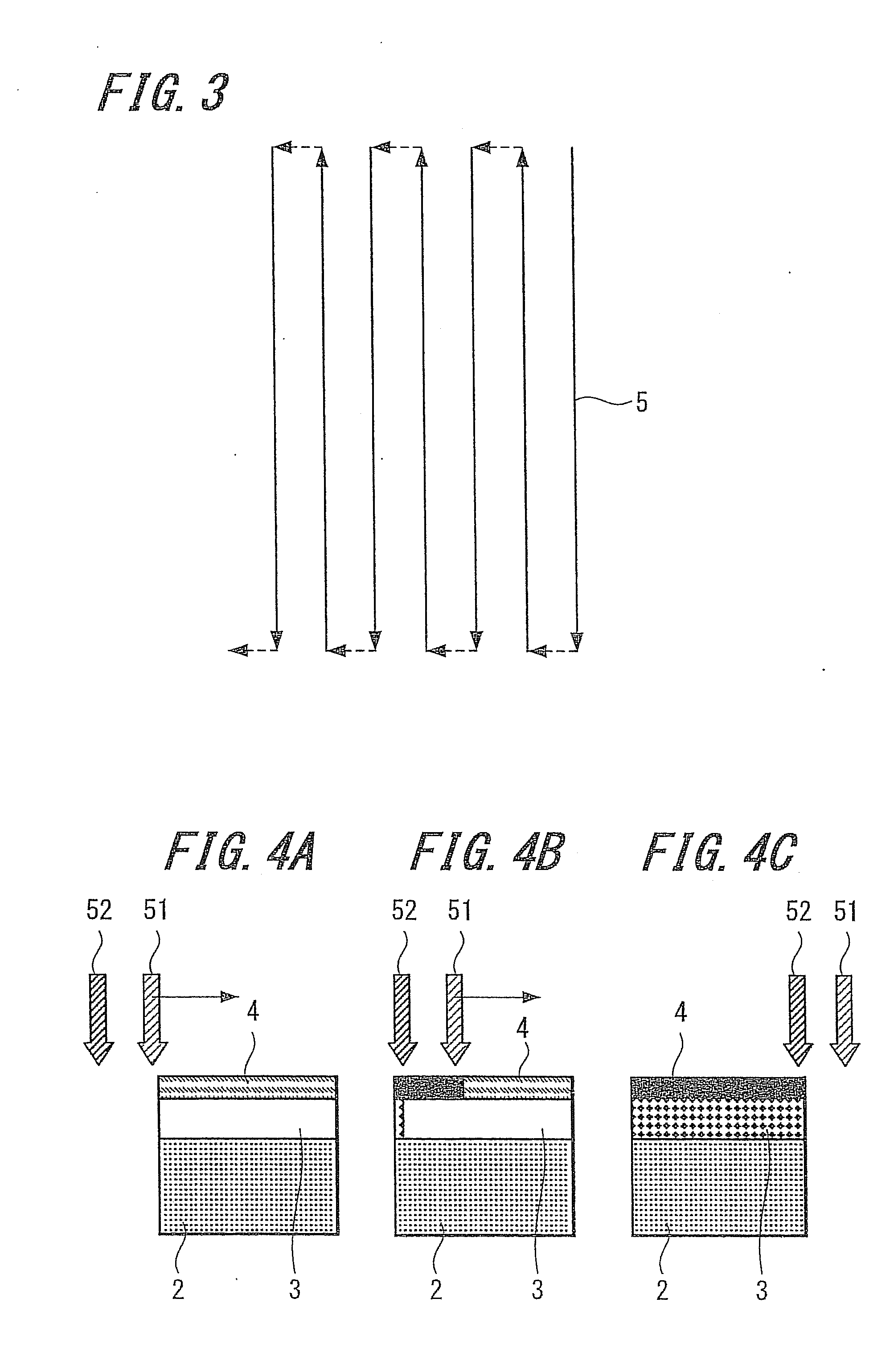
[0042]FIG. 1 shows a schematic cross section of an example of a configuration concerning a heat-treating target body to which the heat-treating method of the present invention is carried out, and herein below, description will be made with respect to the embodiment of the heat-treating method of the present invention.

[0043]In this embodiment, in a heat-treating target body 1, for example a Si semiconductor layer is formed as a heat-treating target layer 3 on a substrate 2, for example a glass substrate, and a light-absorbing layer (also called a heating layer, the same applies herein below) 4 that is based on carbon is further formed thereupon. A heat-transfer layer of 5 nm-100 μm thick can intermediate between the light-absorbing layer 4 and the heat-treating target layer 3, which, however, is not shown in FIG. 1....


PUM


Abstract

The present invention relates to a method of heat-treating a semiconductor, and the object is to enable heat-treating to a semiconductor or semiconductor device in a short period time and to obtain a stable and high reforming effect. The present invention is a method in which carbon or a layer including carbon is provided as a light absorbing layer, and a semiconductor material as a heat-treating target layer or semiconductor device contacting the heat absorbing layer directly or through a heat transfer layer of 5 nm-100 μm in thickness is heat-treated, and the light source to be used is a semiconductor laser light of wavelength of 600 nm-2 μm, and this semiconductor laser light is caused to continuously irradiate and sweep the surface of the heat-treating target material. The light source can be easily made to output high power, and heat-treating at a high speed and with low energy consumption is realized.

Description

TECHNICAL FIELD[0001]The present invention relates to a method of heat-treating materials to be processed, and in particular relates to a method of heat-treating semiconductor materials and devices efficiently in a short period of time.BACKGROUND ART[0002]In manufacture of semiconductor devices, such as various types of semiconductor elements including bipolar transistors and insulated gate field effect transistors (MOS-type transistors), semiconductor integrated circuits, etc., heat-treating is often carried out, for example in repairing crystal defects of a semiconductor, activating introduced impurities, phase-changing from an amorphous material to a crystal, etc.[0003]In particular, for a thin-film transistor that is formed on an insulating body or insulating film, the crystallization technology therefore is important. As conventional thin-film crystallization techniques, a method of heating at a high temperature from 600° C. to 1000° C. for 2 to 20 hours has been known (see, fo...

Claims


Application Information

Patent Timeline
IPC IPC(8): H01L21/268
CPCH01L21/02381H01L21/02683H01L27/1285H01L21/268H01L21/324H01L21/02691H01L21/20
Inventor SANO, NAOKISAMESHIMA, TOSHIYUKI
Owner HIGHTEC SYST CORP
Why Eureka
Try Eureka