Magnetic memory element and magnetic memory device

a magnetic memory and memory layer technology, applied in the direction of magnetic field-controlled resistors, magnetic-on-the-semiconductor devices, electrical devices, etc., can solve the problems of not contributing substantially to the magnetization inversion of the memory layer, the magnetic characteristics of the peripheral part of the memory layer are sometimes deteriorated, and the center part cannot be inverted in some cases, so as to achieve good magnetic characteristics

Active Publication Date: 2009-10-22
RENESAS ELECTRONICS CORP
View PDF3 Cites 6 Cited by
  • Summary
  • Abstract
  • Description
  • Claims
  • Application Information

AI Technical Summary

Benefits of technology

[0014]The present invention thus provides a magnetic memory element and a magnetic memory device

Problems solved by technology

Further, since the inversion energy of the magnetization in the center part of the memory layer is high as compared with that in the peripheral part, even if the magnetization is inverted in the peripheral part, the magnetization cannot be inverted in the center part in some cases.
Furthermore, the magnetic characteristics in the

Method used


Image

  • Magnetic memory element and magnetic memory device
  • Magnetic memory element and magnetic memory device
  • Magnetic memory element and magnetic memory device

Examples


embodiment 1

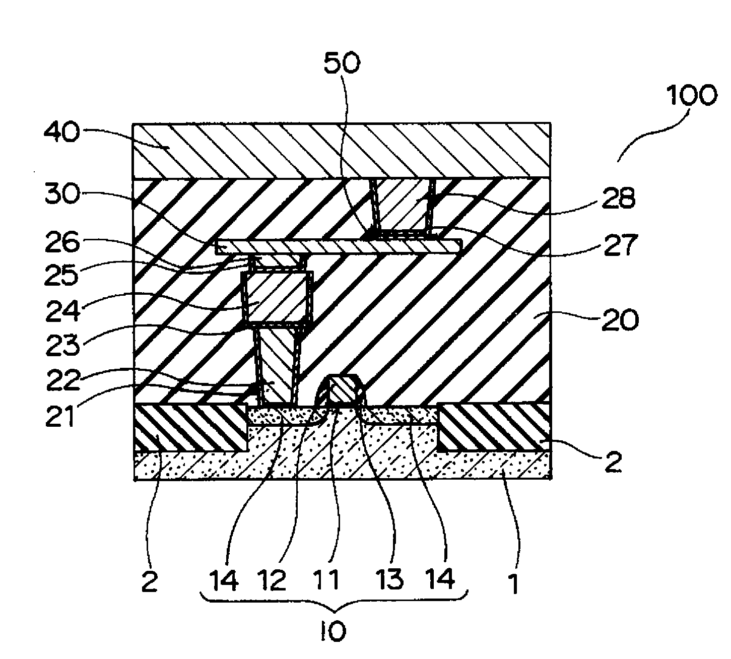
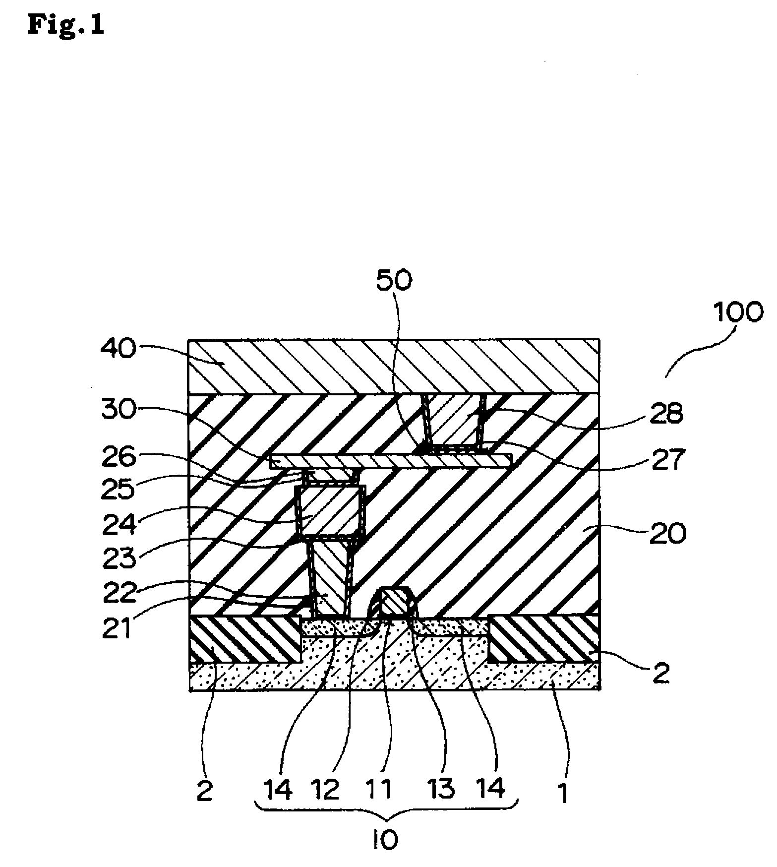
[0023]FIG. 1 shows a partial cross-sectional view of a magnetic memory device (STT-MRAM) (Spin Transfer Torque-MRAM) according to the embodiment of which the entire body is denoted with 100.

[0024]The magnetic memory device 100 contains a semiconductor substrate 1 of silicon or the like. An element separation insulating film 2 of silicon oxide or the like is formed in the semiconductor substrate 1. A transistor 10 for selecting elements is formed in the element formation region separated by the element separation insulating film 2. The transistor 10 contains a gate insulating layer 11 formed on the semiconductor substrate 1 and a gate electrode 12 formed thereon. A side wall 13 of silicon oxide or the like is formed in both sides of the gate electrode 12. A source / drain region 14 is formed in the semiconductor substrate 1 in a manner that the gate electrode 12 is sandwiched.

[0025]An interlayer insulating layer 20 of, for example, silicon oxide is formed on the semiconductor substrate...

embodiment 2

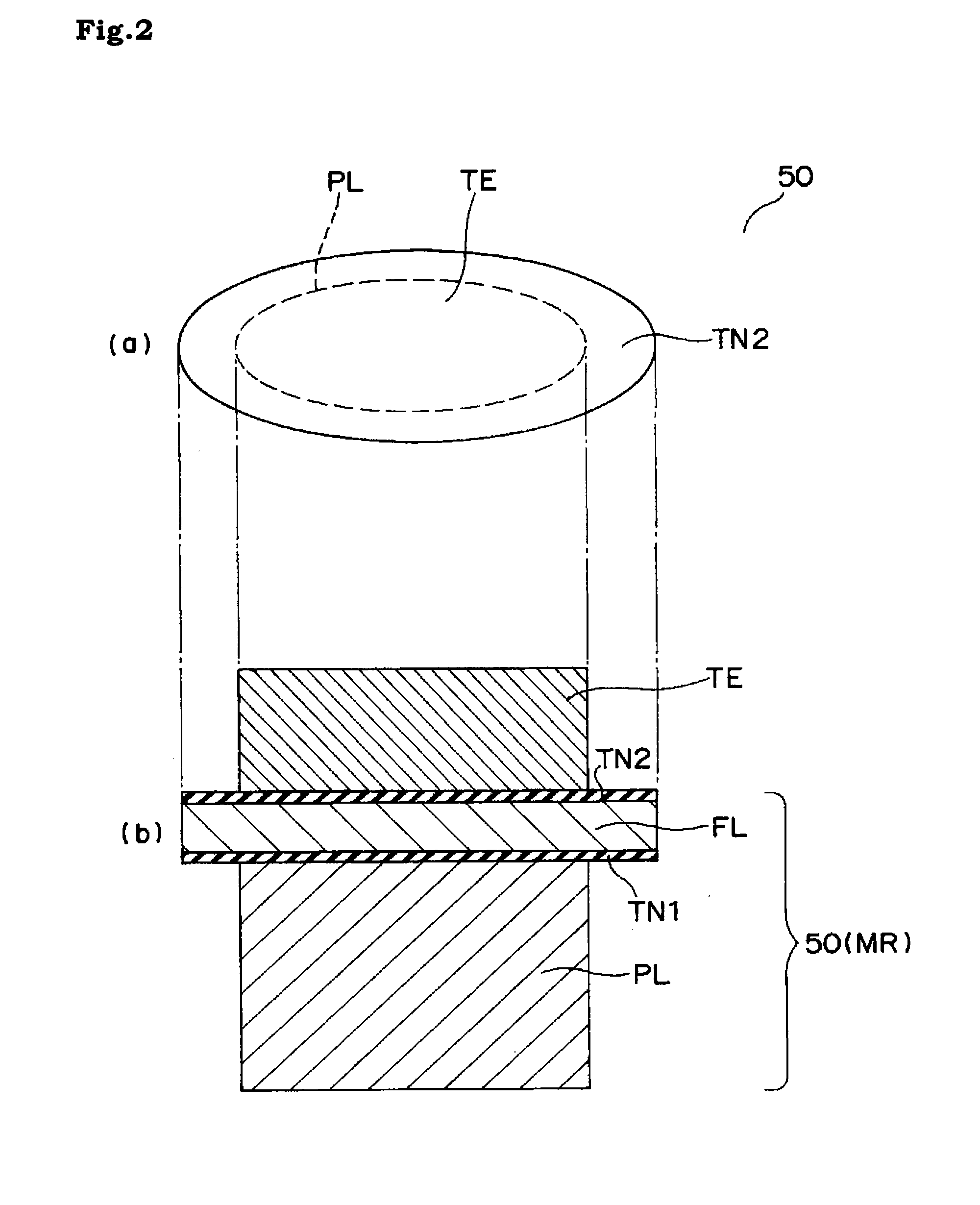
[0045]FIG. 5 show a magnified drawing of another magnetic memory element of the embodiment 2 of which the entire body is denoted as 150 and FIG. 5(a) shows a top drawing and FIG. 5(b) shows a cross-sectional view. In FIG. 5, the symbols same as those in FIGS. 1 and 2 show the same or equivalent parts.

[0046]The magnetic memory element 150 contains a fixing layer (PL) connected with a lead-out electrode 30. On the fixing layer (PL), a tunnel insulating layer (TN1) of a nonmagnet (dielectric), a memory layer (FL) of a ferromagnet, and a top electrode (TE) are successively layered.

[0047]In the magnetic memory element 150 of this embodiment 2, the end part of the fixing layer (PL) is arranged in the inner side than the end part of the tunnel insulating layer (TN1). Further, the distance between the end part of the fixing layer (PL) and the end part of the memory layer (FL) is preferable to be equal to or more than the thickness of the memory layer (FL). On the other hand, the top electro...

embodiment 3

[0050]FIG. 6 show a magnified drawing of a magnetic memory element of the embodiment 3 of which the entire body is denoted as 250 and FIG. 6(a) shows a top drawing and FIG. 6(b) shows a cross-sectional view. In FIG. 6, the symbols same as those in FIGS. 1 and 2 show the same or equivalent parts.

[0051]The magnetic memory element 250 of the embodiment 3 has a structure formed reversely upside down to that of the magnetic memory element 150 of the embodiment 2.

[0052]That is, a memory layer (FL) and a tunnel insulating layer (TN1) are formed on a bottom electrode (BE) (equivalent to the lead-out layer 30 in FIG. 1) and a fixing layer (PL) is formed thereon. The end part of the fixing layer (PL) is arranged in the inner side than the end parts of the memory layer (FL) and the tunnel insulating layer (TN1). Further, the distance between the end part of the fixing layer (PL) and the end part of the memory layer FL is preferable to be equal to or more than the thickness of the memory layer ...


PUM


Abstract

A magnetic memory element having a layer structure containing a fixing layer (pinned layer: PL) having a magnetization direction fixed unidirectionally, a nonmagnetic dielectric layer (TN1) in contact with the fixing layer (PL), and a memory layer (free layer: FL) having a first surface in contact with the nonmagnetic dielectric layer (TN1) and a second surface on the opposite to the first surface, the magnetization direction of the memory layer (FL) having a reversible magnetization direction in response to the current through the layer structure. The entire surface of the first surface of the memory layer (FL) is covered with the nonmagnetic dielectric layer (TN1) and in the joint surface of the nonmagnetic dielectric layer (TN1) and the fixing layer (PL), the first surface of the nonmagnetic dielectric layer (TN1) is exposed in a manner of surrounding the joint surface.

Description

CROSS-REFERENCE TO RELATED APPLICATION[0001]The disclosure of Japanese Patent Application No. 2008-111080 filed on Apr. 22, 2008 including specification, drawings and claims is incorporated herein by reference in its entirely.BACKGROUND OF THE INVENTION[0002]1. Field of the Invention[0003]The present invention relates to a magnetic memory element and a magnetic memory device, particularly a magnetic memory element and a magnetic memory device capable of rewriting information by flowing spin-polarized electrons to the magnetic element.[0004]2. Description of the Related Art[0005]As a nonvolatile magnetic memory device of the next generation, a MRAM (Magnetic Random Access Memory) device has drawn attention. The MRAM device is a nonvolatile magnetic memory device which can store nonvolatile data using a plurality of memory cells of thin film magnetic layers formed in a semiconductor integrated circuit and at the same time which allows random access to the respective memory cells.[0006...

Claims


Application Information

Patent Timeline
IPC IPC(8): H01L29/82
CPCH01L43/08H01L27/228H10B61/22H10N50/10
Inventor TAKADA, HIROSHITAKENAGA, TAKASHIKUROIWA, TAKEHARUFURUKAWA, TAISUKE
Owner RENESAS ELECTRONICS CORP
Why Eureka
Try Eureka