

Thin film structures with negative inductance and methods for fabricating inductors comprising the same
a thin film structure and negative self-inductance technology, applied in the field of passive electronic devices, can solve the problems of eliminating self-inductance, parasitic inductance of high-speed integrated circuits and semiconductor devices, and field able to adversely affect voltage stability,
- Summary
- Abstract
- Description
- Claims
- Application Information
AI Technical Summary
Benefits of technology
Problems solved by technology
Method used
Image

Examples
example 1
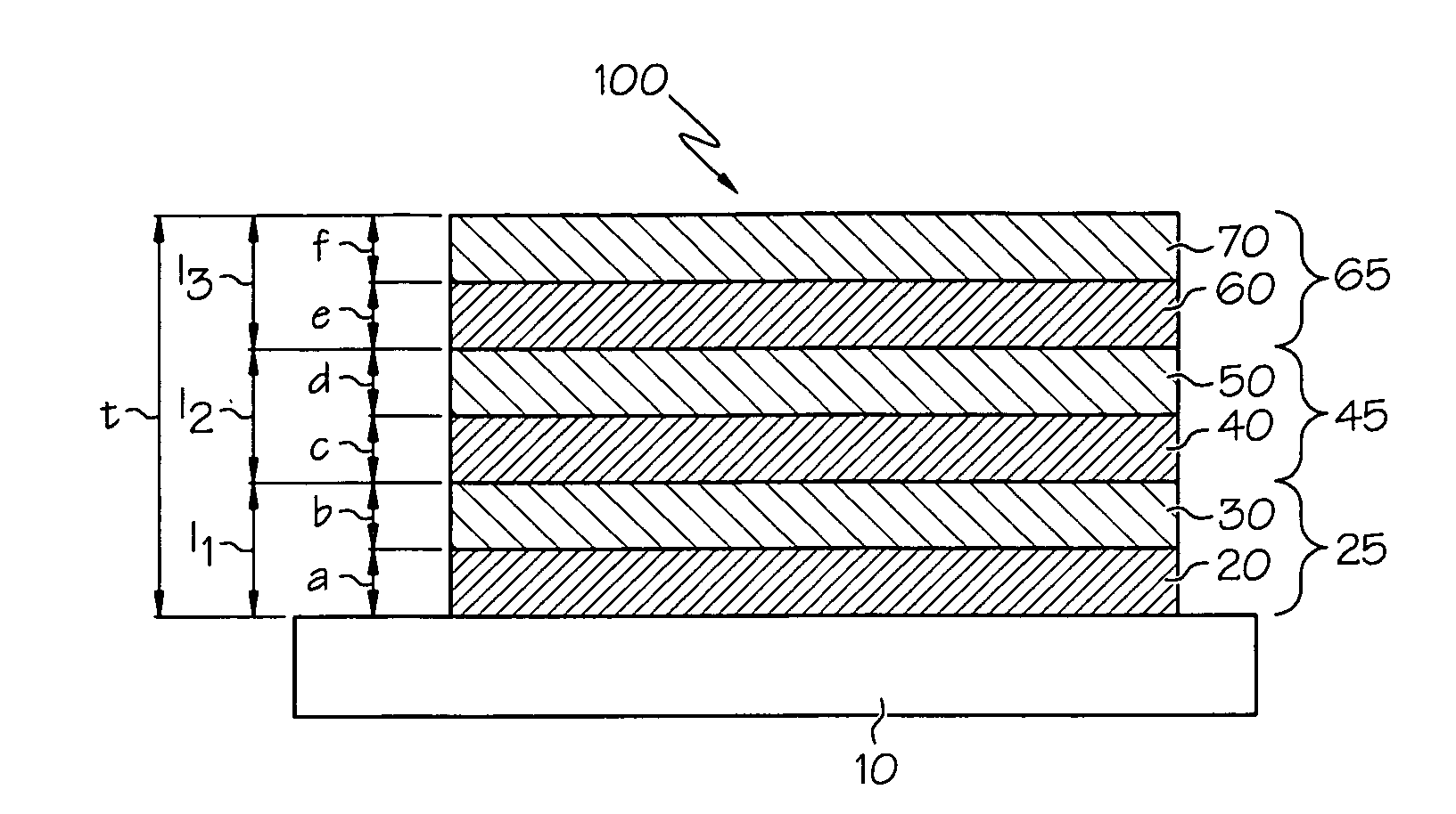
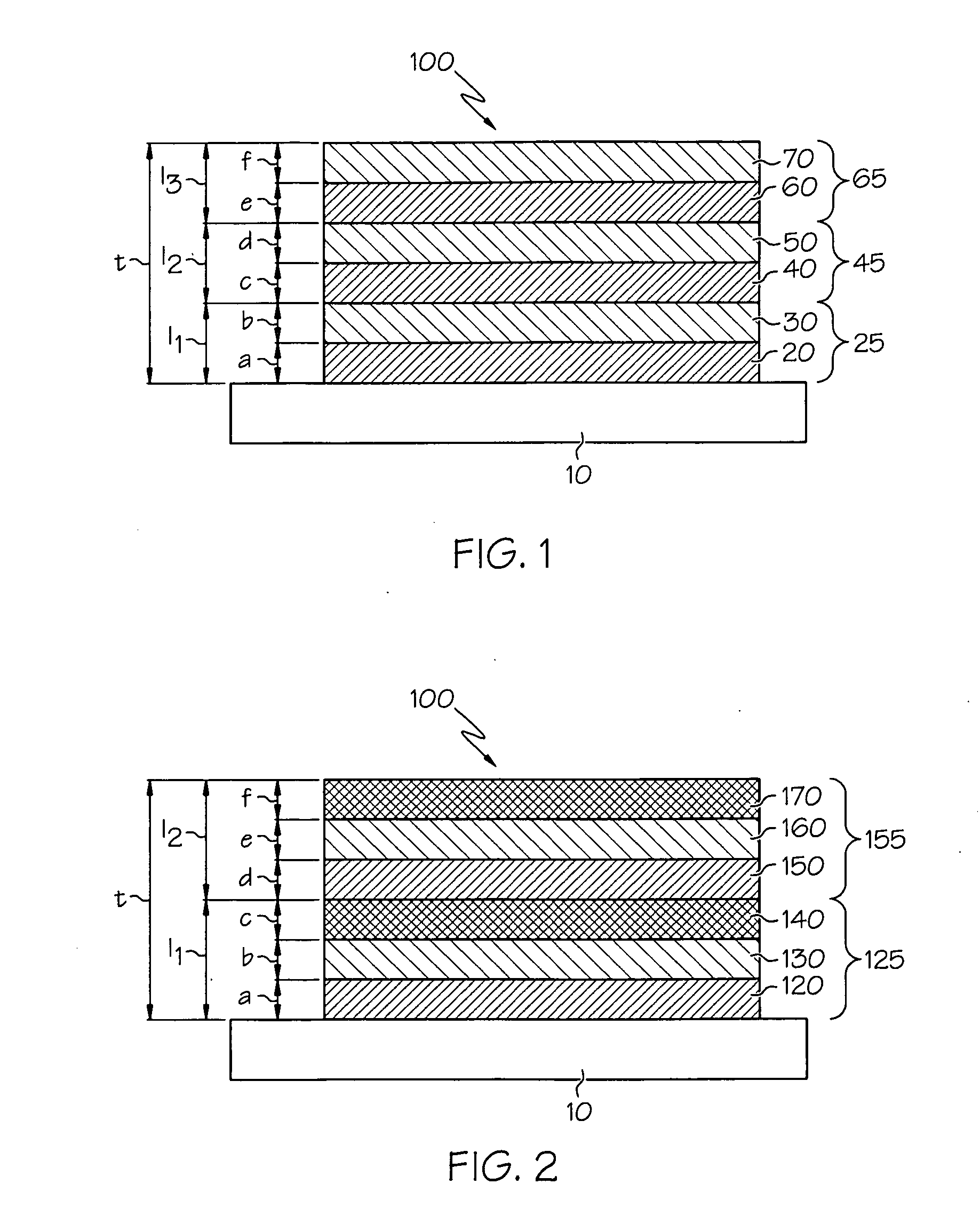
[0053]To examine negative inductance behavior with respect to variation of layer thickness within multilayers, three exemplary inductors were fabricated. The planar conductor structures of the inductors comprised ten multilayers formed by radio-frequency plasma sputtering. Each multilayer comprised a first layer of aluminum and a second layer of copper. The total thickness of the planar conductor structure was approximately 1.0 μm; thus, each multilayer was about 0.1 μm (1000 Å) thick. Each inductor fabricated in this example will be described by the notation AxBy, wherein A is the first metal, B is the second metal, and x and y are thicknesses of the metal layers in each multilayer, normalized to 100. The subscript notation is otherwise unrelated to chemical composition.
[0054]Thus, a first inductor Al34Cu66 was fabricated with all 333 Å thick aluminum layers and 667 Å thick copper layers, for an Al:Cu thickness ratio of 0.5. A second inductor Al50Cu50 was fabricated with all 500 Å ...
example 2
[0056]Additional 10-turn circle inductors were fabricated that showed exceptional negative inductance characteristics below 10 MHz. Each inductor was fabricated with 10 multilayers and planar conductor structure total thickness of 1.0 μm. Described using the thickness notation from Example 1 above, the following thickness ratios resulted in inductors with negative inductance at most frequencies below 10 MHz: Al66Ni34, Al34Ni66, Cu66Ni34, Cu34Ni66, Al66Ag34, and Al16Ni68Cu16.
example 3
[0057]To examine the negative inductance behavior for a given multilayer composition and thickness ratio with respect to number of multilayers, six inductors were fabricated according to embodiments of the present invention. The inductors comprised 2 to 30 Al66Cu34 multilayers, according to the notation described in Example 1 above. The total thickness of each planar conductor was about 1.0 μm. Thus, the thickness of each multilayer varied with respect to number of multilayers, but the thickness ratio of the aluminum layers to the copper layers in each multilayer was constant. The inductance of these inductors with respect to frequency was calculated using the conversion from S-parameters, as described above. The results are compiled in FIG. 7.
[0058]As the data clearly indicate, negative inductance behavior increases in inductors according to embodiments of the invention at all frequencies below 10 MHz as the number of multilayers increases, with total thickness being held constant....
PUM
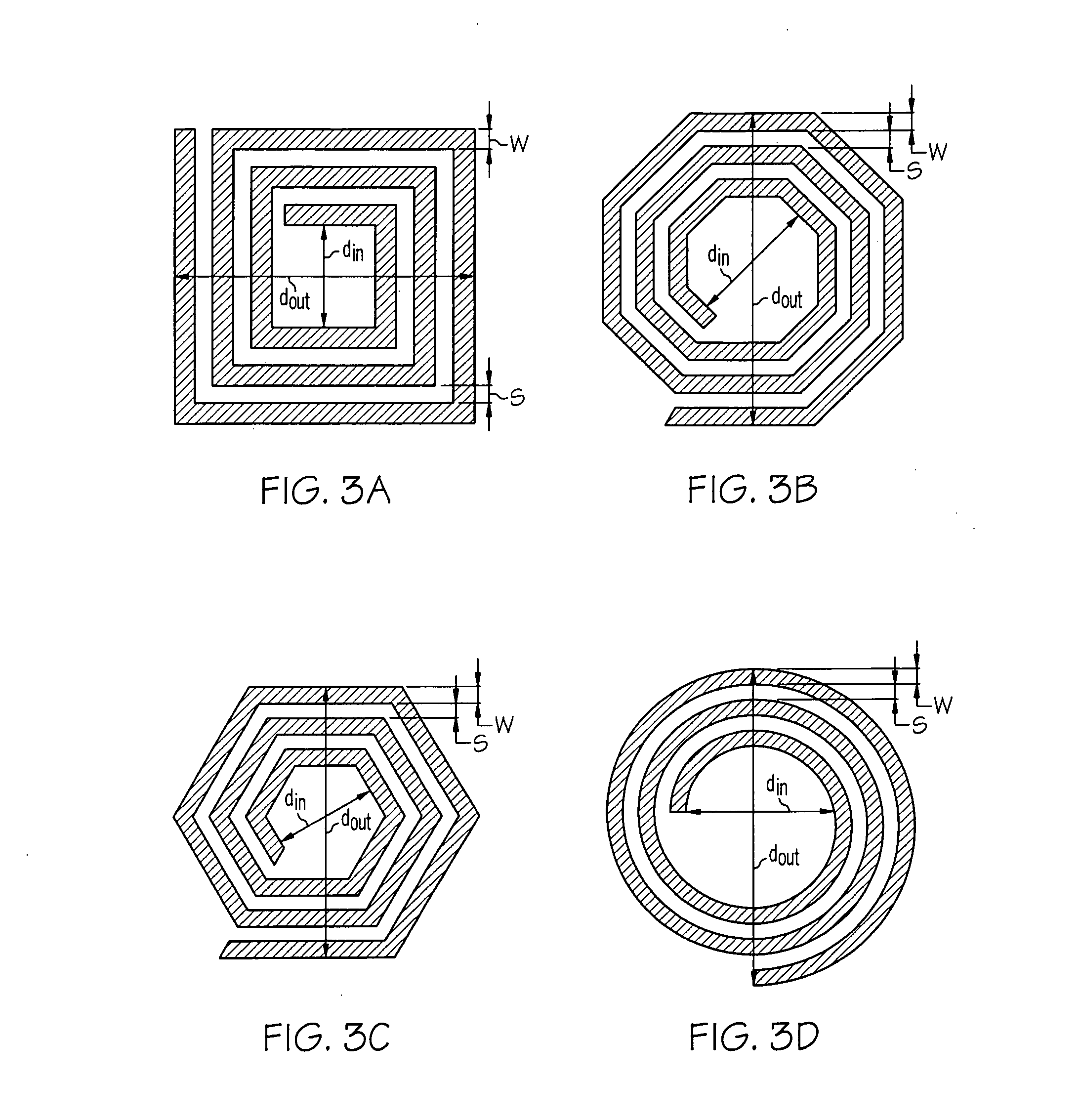
| Property | Measurement | Unit |
|---|---|---|
| frequency | aaaaa | aaaaa |
| frequency | aaaaa | aaaaa |
| inner radius | aaaaa | aaaaa |
Abstract
Description
Claims
Application Information