
Apparatus for sputtering and a method of fabricating a metallization structure

Active Publication Date: 2009-10-22
EVATEC
View PDF8 Cites 12 Cited by
  • Summary
  • Abstract
  • Description
  • Claims
  • Application Information

AI Technical Summary

Benefits of technology

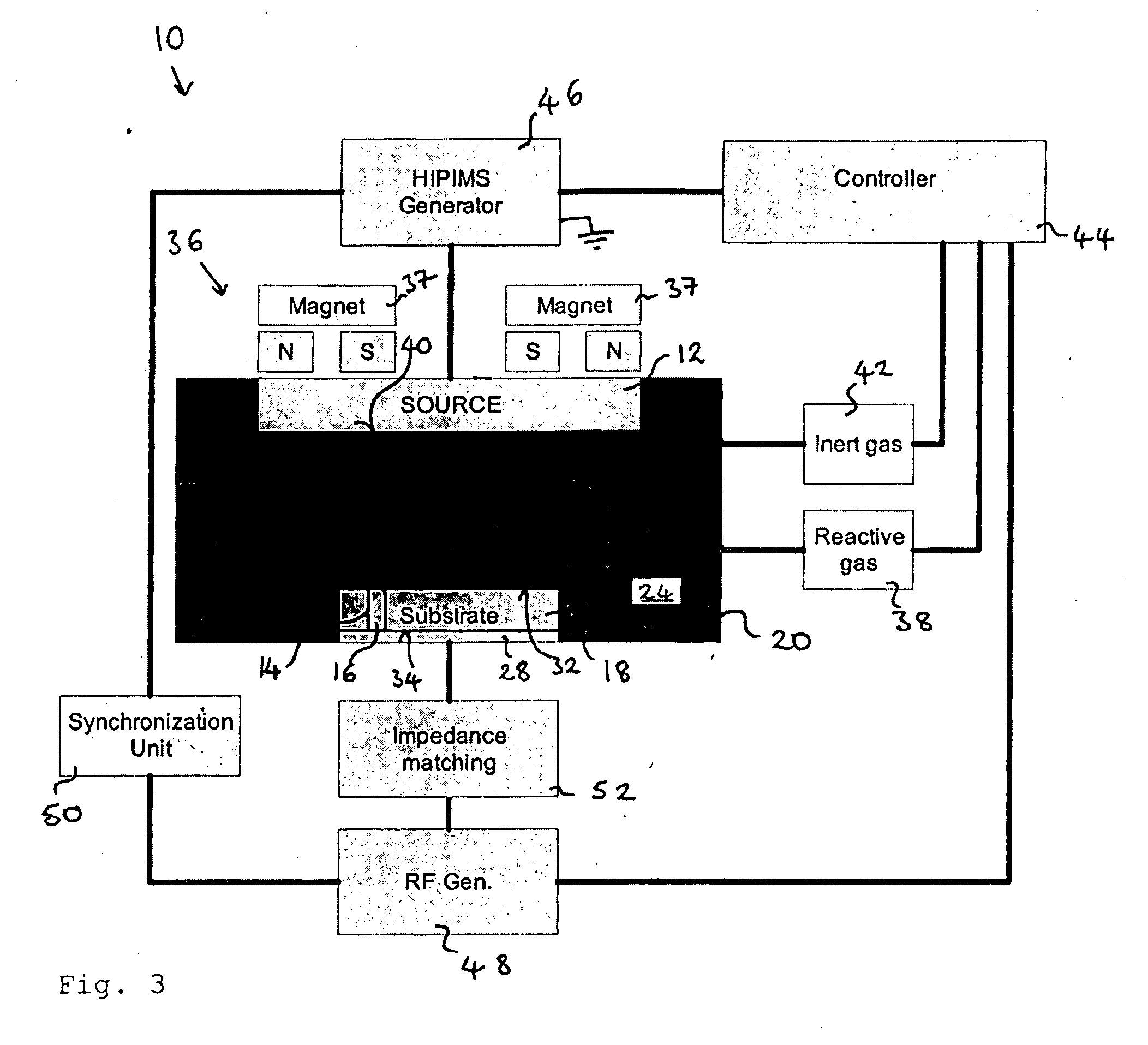
[0014]This method of operating apparatus for high power impulse magnetron sputtering enables an alpha-tantalum layer to be deposited on a TaN layer having a thickness of less than 5 nm and even a thickness of 1 nm and 0.2 nm. The TaN layer is reactively sputter deposited using a pulsed technique. This TaN layer deposited using this method appears to encourage the growth of alpha-Ta over beta-Ta in the overlying Ta layer and encourage the growth of a low resistivity metallization structure. The first power supply may be a DC power supply.

Problems solved by technology

However, high aspect ratios make it difficult to cover the side walls of the via with a layer of material which has a uniform thickness over the side walls.
However, copper has the disadvantage that it diffuses into silicon and, if this occurs, can damage the integrated circuits of the chip and impair its performance.

Method used


Image

  • Apparatus for sputtering and a method of fabricating a metallization structure
  • Apparatus for sputtering and a method of fabricating a metallization structure
  • Apparatus for sputtering and a method of fabricating a metallization structure

Examples


example 1

[0083]The process listed in table 2 was sputtered at a process pressure of 3.9×10⁻⁶ bar. RF-Bias of 50 V was applied, although not required for the deposition of the TaN seed layer. The further deposition conditions are summarized in table 2.

[0084]A specific resistivity of 23 μΩcm was measured by a four point-probe mapping system for this film. Together with the XRD peak at 2 theta=38.472° illustrated in FIG. 13 which can be assigned to the (1 1 0) peak of tantalum, the crystallographic phase of example 1 was characterized as the alpha (bcc) Ta.

example 2

[0085]In the following example the TaN seed layer thickness was varied. If HIPIMS is used, the TaN seed layer can be reduced to a minimum of 0.2 nm. The deposition conditions are summarized in table 3.

[0086]For a 7.5 nm seed layer we sputtered 15 s with 500 Hz. By reducing the sputtering time to 10 s and 5 s we deposited TaN layers of 5 nm and 2.5 nm. In order to decrease the thickness to 1.25 nm the pulse frequency was halved from 500 Hz to 250 Hz by leaving the sputtering time at 5 s. We deposited a TaN layer of 0.5 nm by applying a flash of N2 into the process chamber for with a pulse frequency of 500 Hz. Finally, a thickness of approximately 0.2 nm by sputtering for 2 s with a frequency of 250 Hz.

[0087]FIG. 14 illustrates the specific resistivity of 600 nm alpha-Ta layers deposited on different TaN seed layer thicknesses in the range 7.5 nm to 0.2 nm. For TaN seed layer thicknesses of 7.5 nm to 0.5 nm, the resistivity of the tantalum layer remained below 20 μΩcm. The resistivity...


PUM

PropertyMeasurementUnit
Fractionaaaaaaaaaa
Fractionaaaaaaaaaa
Thicknessaaaaaaaaaa

Abstract

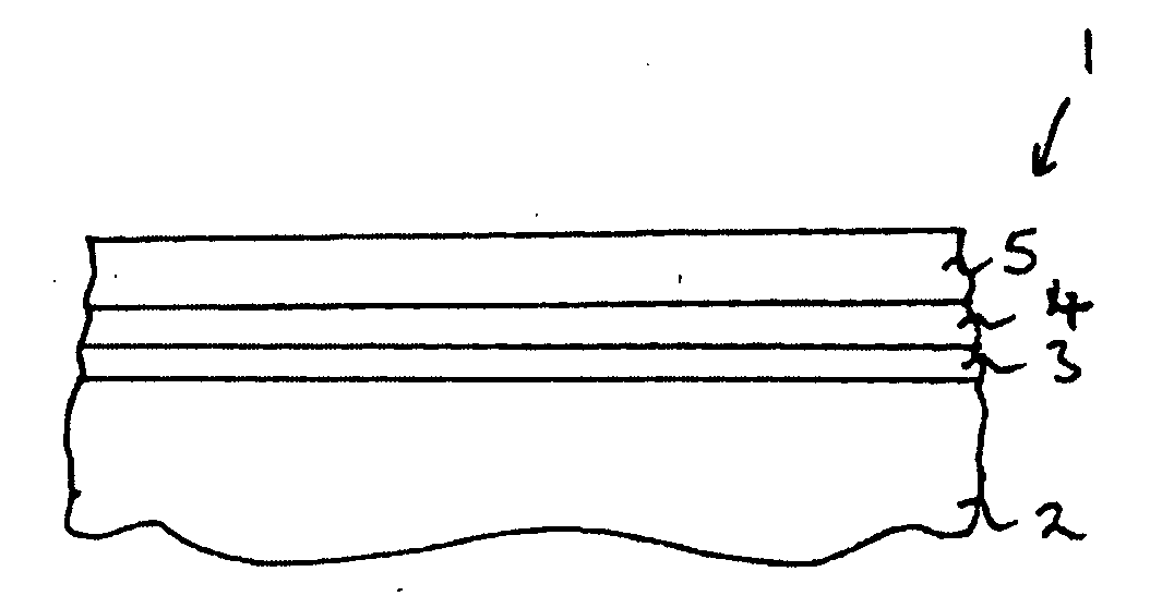
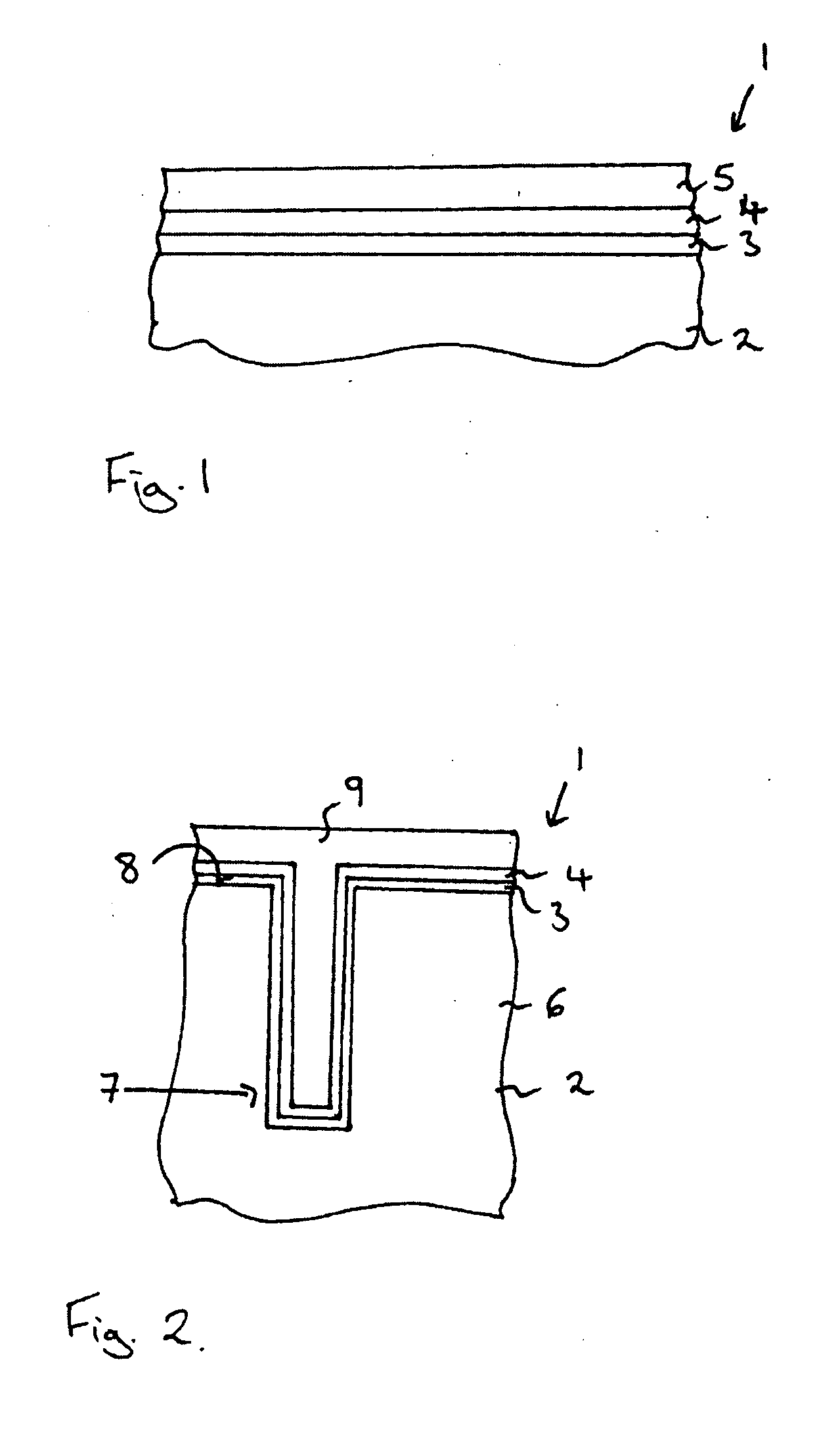
A method of depositing a metallization structure (1) comprises depositing a TaN layer (4) by applying a power supply between an anode and a target in a plurality of pulses to reactively sputter Ta from the target onto the substrate (2) to form a TaN seed layer (4). A Ta layer (5) is deposited onto the TaN seed layer (4) by applying the power supply in a plurality of pulses and applying a high-frequency signal to a pedestal supporting the substrate (2) to generate a self-bias field adjacent to the substrate (2).

Description

FIELD OF THE INVENTION[0001]The present application relates to apparatus for sputtering and to a method of fabricating a metallization structure, in particular, a metallization structure for a semiconductor chip.BACKGROUND OF THE INVENTION[0002]Semiconductor chips face constant development aimed at increasing the performance of the circuits supported by the chips while decreasing the overall physical size of the chips. Physical limitations like power dissipation in integrated circuits (IC's) and the process technology for fabricating IC's on an ever smaller scale have recently encouraged vertically stacking a plurality of chips instead of further increasing the lateral device density to enhance performance.[0003]Semiconductor chips which are to be vertically stacked may be fabricated to include through silicon vias to establish electrical connections between the vertically stacked semiconductor chips. The through silicon vias are typically high aspect ratio holes in the semiconducto...

Claims


Application Information

Patent Timeline
IPC IPC(8): H01L21/3205C23C14/35C23C14/38
CPCC23C14/046C23C14/0641C23C14/165C23C14/3485H01J37/3467H01L21/2855C23C14/35H01J37/345H01L21/76843H01L23/53238C23C14/3407C23C14/345C23C14/50
Inventor WEICHART, JUERGENELGHAZZALI, MOHAMEDBAMMESBERGER, STEFANMINKOLEY, DENNIS
Owner EVATEC
Learn More