Mosfet device having dual interlevel dielectric thickness and method of making same

a technology of dielectric thickness and mosfet, which is applied in the direction of mosfet devices, basic electric elements, electrical appliances, etc., can solve the problems of reduced transconductance, increased threshold voltage of devices, and reduced device performance, so as to reduce hot carrier injection

Inactive Publication Date: 2009-10-29
CICLON SEMICON DEVICE
View PDF32 Cites 26 Cited by
  • Summary
  • Abstract
  • Description
  • Claims
  • Application Information

AI Technical Summary

Benefits of technology

[0005]A method of forming a metal-oxide-semiconductor (MOS) device is provided where the thicknesses of the interlevel dielectric layers of the MOS device can be ind

Problems solved by technology

The electrons remain trapped in the gate oxide resulting in a decrease in device performance including, but not limited to, an increase in the threshold voltage of the device and a reduction in transconductance.
One disadvantage of the dummy gate approach shown in FIG. 1 to reducing hot carrier injection effect is the inability to optimize the interlevel dielectric

Method used


Image

  • Mosfet device having dual interlevel dielectric thickness and method of making same
  • Mosfet device having dual interlevel dielectric thickness and method of making same
  • Mosfet device having dual interlevel dielectric thickness and method of making same

Examples


Embodiment Construction

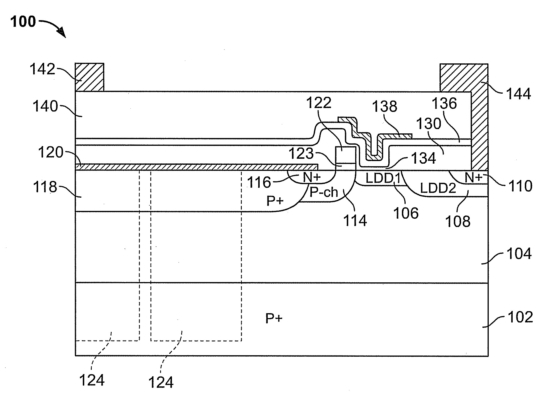
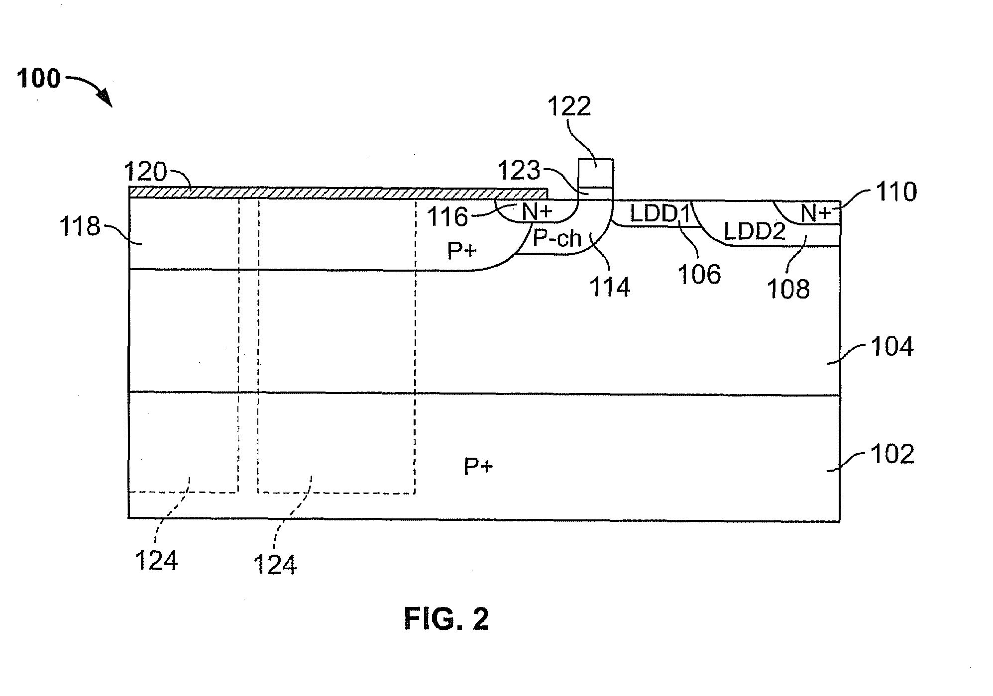
[0011]As used herein, the following dopant concentrations are distinguished using the following notations: (a) N++ or P++: dopant concentration of 5×10¹⁹ atoms / cm3 and greater; (b) N+ or P+: dopant concentration of 1×10¹⁸ to 5×10¹⁹ atoms / cm3; (c) N or P: dopant concentration of 5×10¹⁶ to 1×10¹⁸ atoms / cm3; (d) N− or P−: dopant concentration of 1×10¹⁵ to 5×10¹⁶ atoms / cm3; (e) N−− or P−−: dopant concentration 15 atoms / cm3.

[0012]It should be appreciated that, in the case of a simple MOS device, because the MOS device is symmetrical in nature, and thus bidirectional, the assignment of source and drain designations in the MOS device is essentially arbitrary. Therefore, the source and drain regions may be referred to generally as first and second source / drain regions in some cases, respectively, where “source / drain” in this context denotes a source region or a drain region. In an LDMOS device, which is generally not used in a bidirectional mode, such source and drain designations may not b...


PUM


Abstract

A method of forming a metal-oxide-semiconductor (MOS) device includes the following steps: forming a semiconductor layer of a first conductivity type having source and drain regions of a second conductivity type, a channel region and a lightly-doped drain region formed therein; forming a gate over the channel region proximate an upper surface of the semiconductor layer; after the forming steps, depositing a first dielectric layer having a first thickness over an upper surface of the semiconductor layer; etching the first dielectric layer in a region over the lightly-doped drain proximate to the gate to reduce its thickness; conformably depositing a second dielectric layer having a second thickness over the first dielectric layer, including in the etched region, the second thickness being less than the first thickness; and forming a shielding electrode over the second dielectric layer.

Description

FIELD OF THE INVENTION[0001]The present invention relates to semiconductor devices and methods of making the same and more particularly to laterally diffused MOS (LDMOS) transistor devices and methods of making the same.BACKGROUND OF THE INVENTION[0002]The device performance of MOS devices can be degraded by a phenomenon known as “hot carrier injection” or HCI where the electric field from the drain acts in a manner close to the gate structure to aid the injection of electrons from the active channel of the device into the gate oxide. The electrons remain trapped in the gate oxide resulting in a decrease in device performance including, but not limited to, an increase in the threshold voltage of the device and a reduction in transconductance.[0003]One common method of mitigating the effect of hot carrier injection is to use a dummy gate structure. In this approach, an interlevel dielectric layer is deposited over the active gate and a dummy gate structure is placed on top of the int...

Claims


Application Information

Patent Timeline
IPC IPC(8): H01L29/78H01L21/336
CPCH01L29/0847H01L29/7835H01L29/66659H01L29/402
Inventor PEARCE, CHARLES WALTERMOLLOY, SIMON J.XU, SHUMINGLI, XIAO RUI
Owner CICLON SEMICON DEVICE
Why Eureka
Try Eureka