

Semiconductor laser apparatus
a laser and semiconductor technology, applied in the direction of laser details, laser optical resonator construction, optical resonator shape and construction, etc., can solve the problem of cost, and achieve the effect of reducing the size of wavelength variable lasers
- Summary
- Abstract
- Description
- Claims
- Application Information
AI Technical Summary
Benefits of technology
Problems solved by technology
Method used
Image

Examples
first embodiment
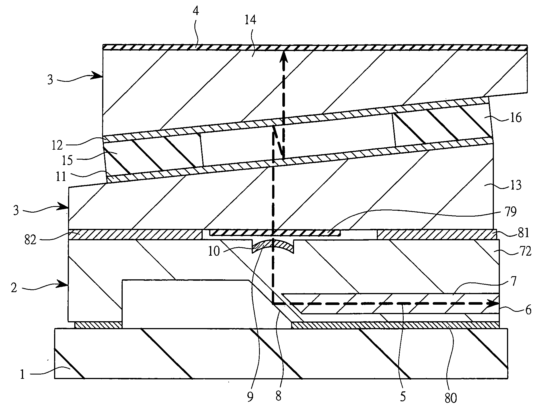
[0046]The first embodiment will be described with reference to FIG. 4 and FIG. 8 to FIG. 11. The first embodiment provides the wavelength variable laser of the 1.55 μm band using a liquid crystal etalon filter. As described above with reference to FIG. 4, the wavelength variable laser according to the first embodiment has a structure in which the gain chip 2, the etalon filter 3 and the reflective mirror 4 are arranged on the AlN submount 1.
[0047]FIG. 8 to FIG. 11 show the structure of the gain chip 2. FIG. 8 is a perspective cross sectional view of the gain chip 2 according to the first embodiment, FIG. 9 is a cross sectional view of the gain chip 2 taken by a plane parallel to the traveling direction of the light, FIG. 10 is a bottom view of the gain chip 2 and FIG. 11 is a cross sectional view of the gain chip 2 taken by a plane orthogonal to the traveling direction of the light, respectively. As shown in FIG. 8 and FIG. 11, an optical waveguide (optical waveguide layer) portion ...
second embodiment
[0060]The second embodiment will be described with reference to FIG. 5 and FIG. 8 to FIG. 11. The second embodiment provides the wavelength variable laser of the 1.55 μm band using a MEMS etalon. The gain chip 2, the MEMS etalon filter and the reflective mirror 4 are arranged on the AlN submount 1.
[0061]The fabrication method of the gain chip 2 of the second embodiment is the same as that of the first embodiment.
[0062]In the MEMS etalon filter according to the second embodiment, the reflective mirrors 11 and 12 are formed on a silicon substrate by the known method. In this case, the reflective mirror 12 is configured to be moved by applied voltage.
[0063]In the wavelength variable laser according to the second embodiment, the single mode oscillation can be caused in a wide wavelength range from 1.53 μm to 1.57 μm by the control of the voltage applied to the MEMS etalon filter and the current injection to the gain multilayer.
[0064]Further, the oscillation wavelength of the wavelength ...
third embodiment
[0065]The third embodiment will be described with reference to FIG. 7 and FIG. 8 to FIG. 11. The third embodiment provides the wavelength variable laser with the wavelength range from 1.53 μm to 1.62 μm using a liquid crystal etalon filter.
[0066]The gain chips 52 and 53, the etalon filter 54 and the reflective mirrors 55 and 56 are arranged on the AlN submount 51. Further, the optical multiplexer 64 formed of the glass substrate 59 and the optical fiber 65 are arranged.
[0067]The fabrication method of the gain chips 52 and 53 of the third embodiment is the same as that of the first embodiment. However, the composition of the InGaAsP active layer is changed so that the gain chip 52 has a gain in the wavelength of 1.53 μm to 1.57 μm and the gain chip 53 has a gain in the wavelength of 1.57 μm to 1.62 μm. The fabrication method of the liquid crystal etalon filter (etalon filter 54) is the same as that of the first embodiment. However, the reflective mirror 55 has a reflectivity of 90% o...
PUM
 Abstract
Description
Claims
Application Information