

Guided-mode-resonance transmission color filters for color generation in CMOS image sensors
a color filter and cmos image sensor technology, applied in the field of cmos imagers, can solve the problems of not being easily integrated with complimentary metal oxide semiconductor (cmos) circuits, charging-coupled devices (ccds), and not being easily adapted to large-scale signal processing
- Summary
- Abstract
- Description
- Claims
- Application Information
AI Technical Summary
Problems solved by technology
Method used
Image

Examples
Embodiment Construction
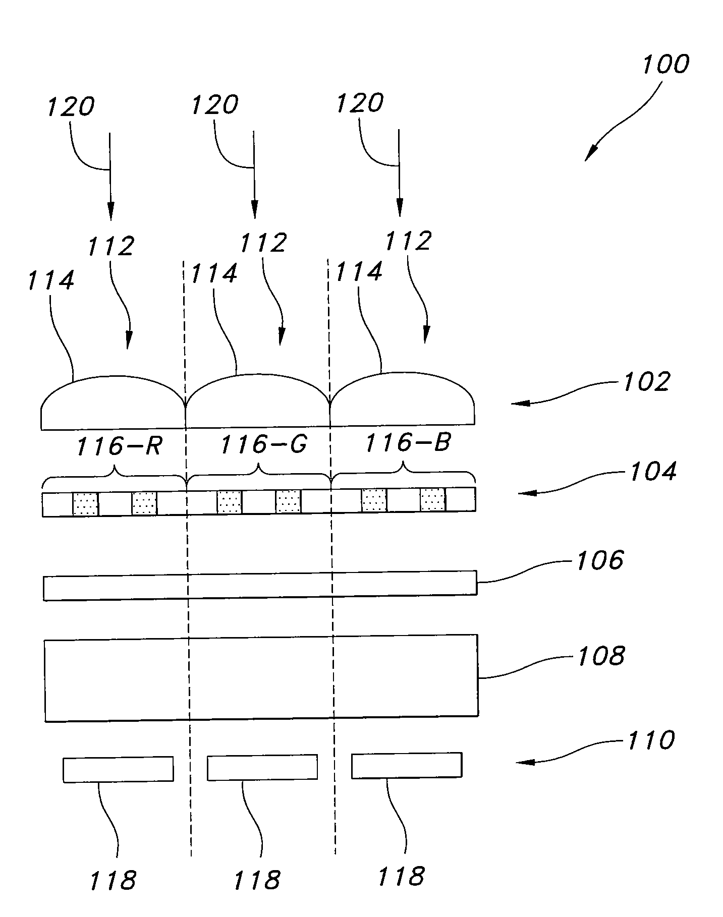
[0015]The term “pixel” as used herein, refers to a photoelement unit cell containing a photosensor device and associated structures for converting photons to an electrical signal. For purposes of illustration, a representative 3 color R,G,B pixel array (representing red, green and blue optical filters) is described herein. The invention, however, is not limited to the use of a R,G,B array and may be used with other optical filter arrays, one example being C,M,Y,K (representing cyan, magenta, yellow and black optical filters). The invention may also be used in a mono-chromatic array where just one color is sensed by the array.
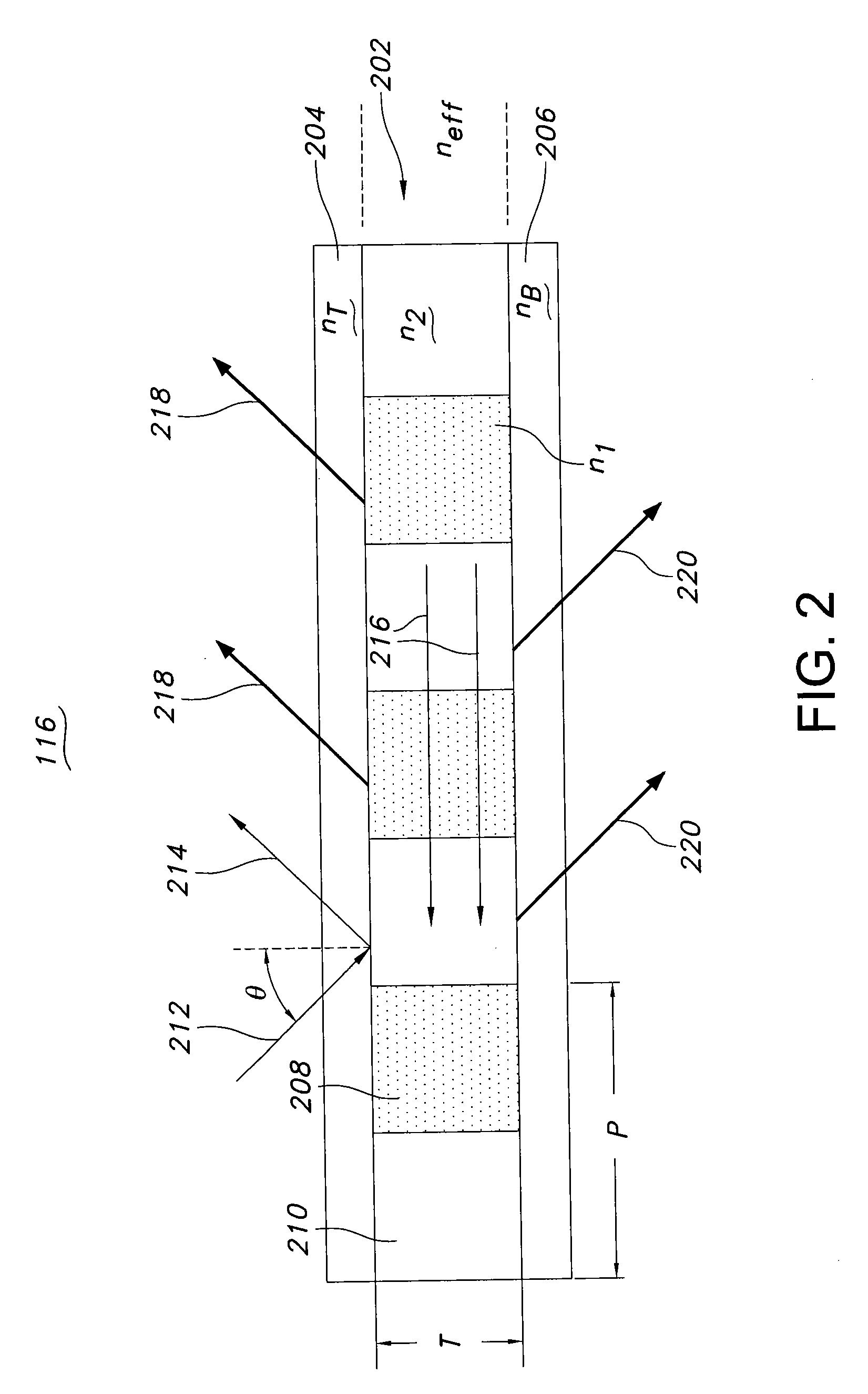
[0016]FIG. 1 is an exploded partial side diagram of imager array 100. Imager array 100 includes microlens array 102 having a plurality of microlenses 114, waveguide grating layer 104 having a plurality of waveguide grating resonance filters 116 and pixel array 110 having a plurality of photosensors 118. Photosensors 118 may include photogates, phototransistors, ...
PUM
 Abstract
Description
Claims
Application Information