Solid-state image pickup apparatus, drive method for the solid-state image pickup apparatus, and image pickup apparatus
- Summary
- Abstract
- Description
- Claims
- Application Information
AI Technical Summary
Benefits of technology
Problems solved by technology
Method used
Image
Examples
embodiment 1
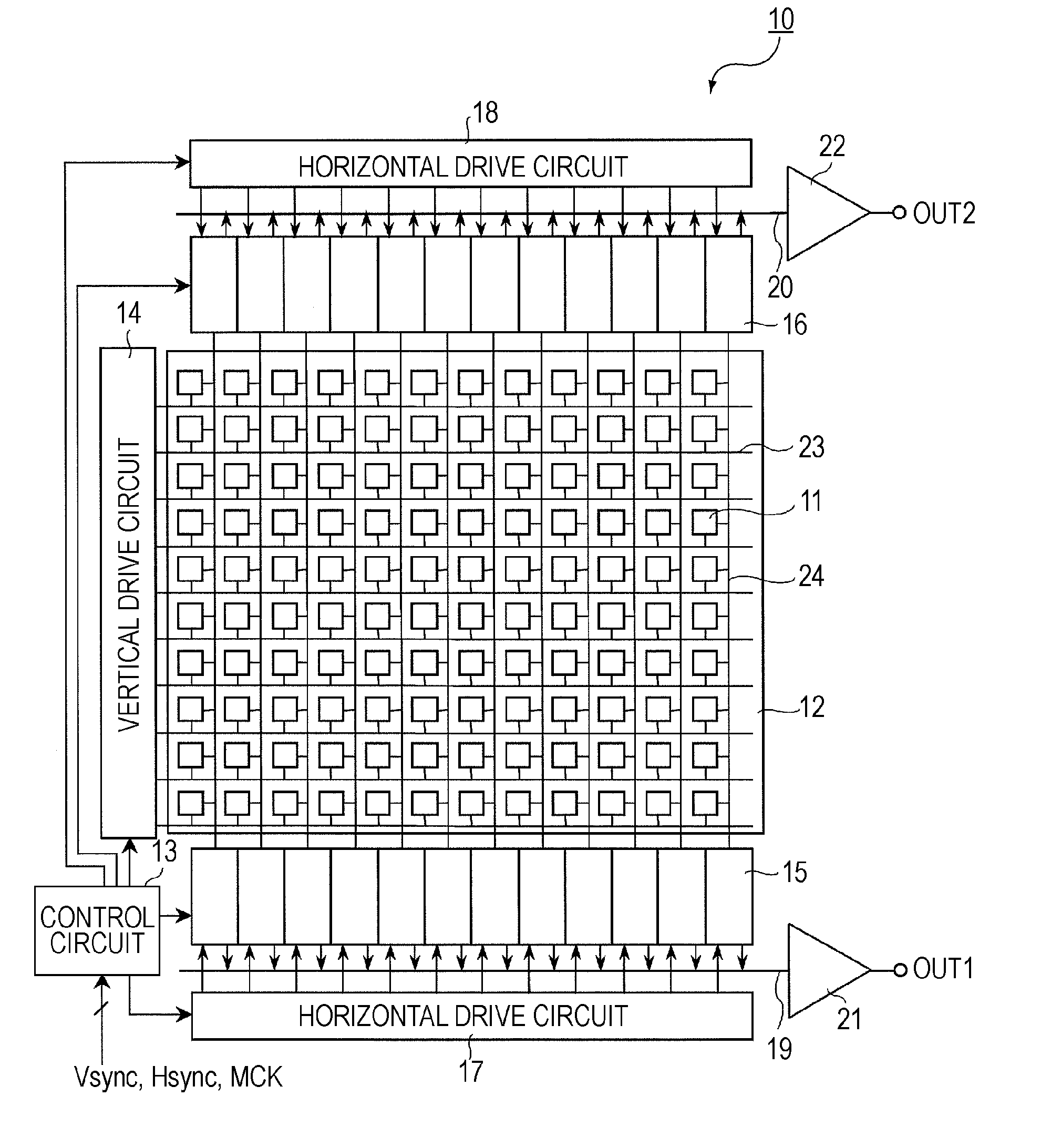
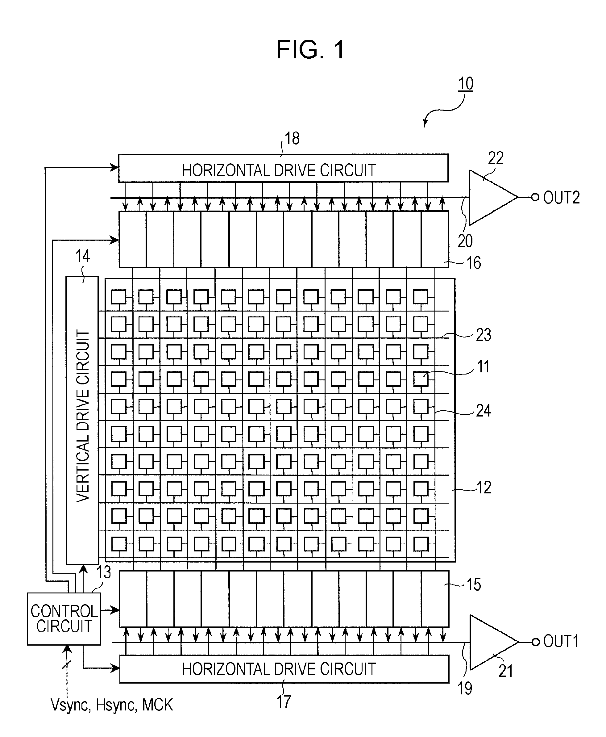
[0076]The signals of the respective pixels on the read row 1 are dealt with as shown in FIG. 5(A). First, the signals are read from the pixels 11, and also the CDS processing is performed. Next, the signals after the CDS processing are amplified at the basis amplification rate (x1) and stored in the latch circuit 154 after the AD conversion. This signal amplified at the basis amplification rate and stored in the latch circuit 154 is set as S1.
[0077]The signals of the respective pixels on the read row 2 are dealt with as shown in FIG. 5(B). First, the signals are read from the pixels 11, and also the CDS processing is performed. Next, the signals after the CDS processing are amplified at 4-fold the basis amplification rate and stored in the latch circuit 164A after the AD conversion. This signal amplified at 4-fold the basis amplification rate and stored in the latch circuit 164A is set as S2. Subsequently, the same signal stored in the CDS circuit 161 is amplified at the basis ampli...
embodiment 2
[0095]In a column signal processing according to Embodiment 2, a method is adopted to simplify the circuit and handing instead of expanding the dynamic range as much as possible. Depending on a product, this method may be more preferable.
[0096]An example of the processing is shown in FIG. 7. Herein, the combination of the read rows 1 and 2 and the column signal processing circuits 15 and 16 is set opposite to Embodiment 1 due to circumstances at the time of the high gain setting. As described above, the combination of the read rows 1 and 2 and the column signal processing circuits 15 and 16 is arbitrary.
[0097]When the gain setting is lower than the predetermined gain, the signals of the respective pixels on the read row 1 are read to the column signal processing circuit 16, and the signals of the respective pixels on the read row 2 are read to the column signal processing circuit 15. Then, either of the column signal processing circuits 15 and 16 is amplified at the basic amplificat...
example 1
CIRCUIT EXAMPLE 1
[0112]FIG. 8 is a circuit diagram showing a column signal processing circuit in which a CDS circuit and an amplification circuit are configured by a general charge voltage conversion amplifier according to Circuit Example 1.
[0113]A charge voltage conversion amplifier 30 constituting a part of the column signal processing circuit according to Circuit Example 1 has a known circuit configuration of having a first switch 31 whose one terminal is connected to the vertical signal lines 24, a second switch 32 connected between the other terminal of the first switch 31 and an arbitrary fixed potential VO, an input capacitance 33 whose input terminal is connected to the other terminal of the first switch 31, a differential amplifier 34 whose inverting (−) input terminal is connected to an output terminal of the input capacitance 33 and in which a clamp voltage Vclp is given to a non-inverting (+) input terminal, a third switch 35 connected between the inverting input termina...
PUM
 Abstract
Description
Claims
Application Information


