Thin Film Transistor

a thin film transistor and film technology, applied in the direction of transistors, semiconductor devices, electrical equipment, etc., can solve the problems of lcd, high manufacturing cost, difficult to apply amorphous silicon to an active matrix oled (amoled), etc., to minimize the occurrence of hysteresis and improve electron mobility

Inactive Publication Date: 2009-11-12
KOREA INST OF SCI & TECH
View PDF4 Cites 151 Cited by
  • Summary
  • Abstract
  • Description
  • Claims
  • Application Information

AI Technical Summary

Benefits of technology

[0009]Example embodiments have been made in an effort to solve the above-described problems associated with the prior art. Example embodiments provide a thin film transistor (TFT) capable of improving electron mobility and minimizing the occurrence of hysteresis due to traps.

Problems solved by technology

When amorphous silicon is used as the channel layer, electron mobility is low, i.e., about 1 cm2 / Vcm or less, and therefore, it is difficult to apply the amorphous silicon to an active matrix OLED (AMOLED), LCD with high mobility or the like.
When the poly-crystalline silicon is used as the channel layer, electron mobility is excellent, but manufacturing cost is high.
At this time, since a large number of traps exist at the interface between the dielectric substance and another thin film layer, electric charges may be trapped in the traps.
If switching operations are performed repeatedly, hysteresis is caused, and as a result, the threshold voltage may be increased.

Method used


Image

  • Thin Film Transistor
  • Thin Film Transistor
  • Thin Film Transistor

Examples


Embodiment Construction

[0030]Hereinafter, reference will be made in detail to various example embodiments of the present invention, examples of which are illustrated in the accompanying drawings and described below. While the invention will be described in conjunction with example embodiments, it will be understood that the present description is not intended to limit the invention to those example embodiments. On the contrary, the invention is intended to cover not only the example embodiments, but also various alternatives, modifications, equivalents and other embodiments, which may be included within the spirit and scope of the invention as defined in the appended claims.

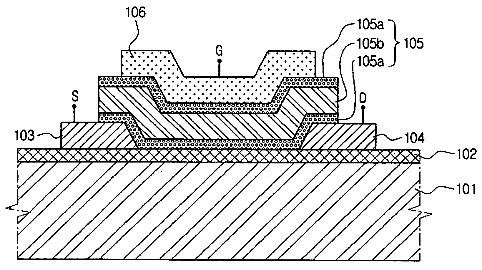
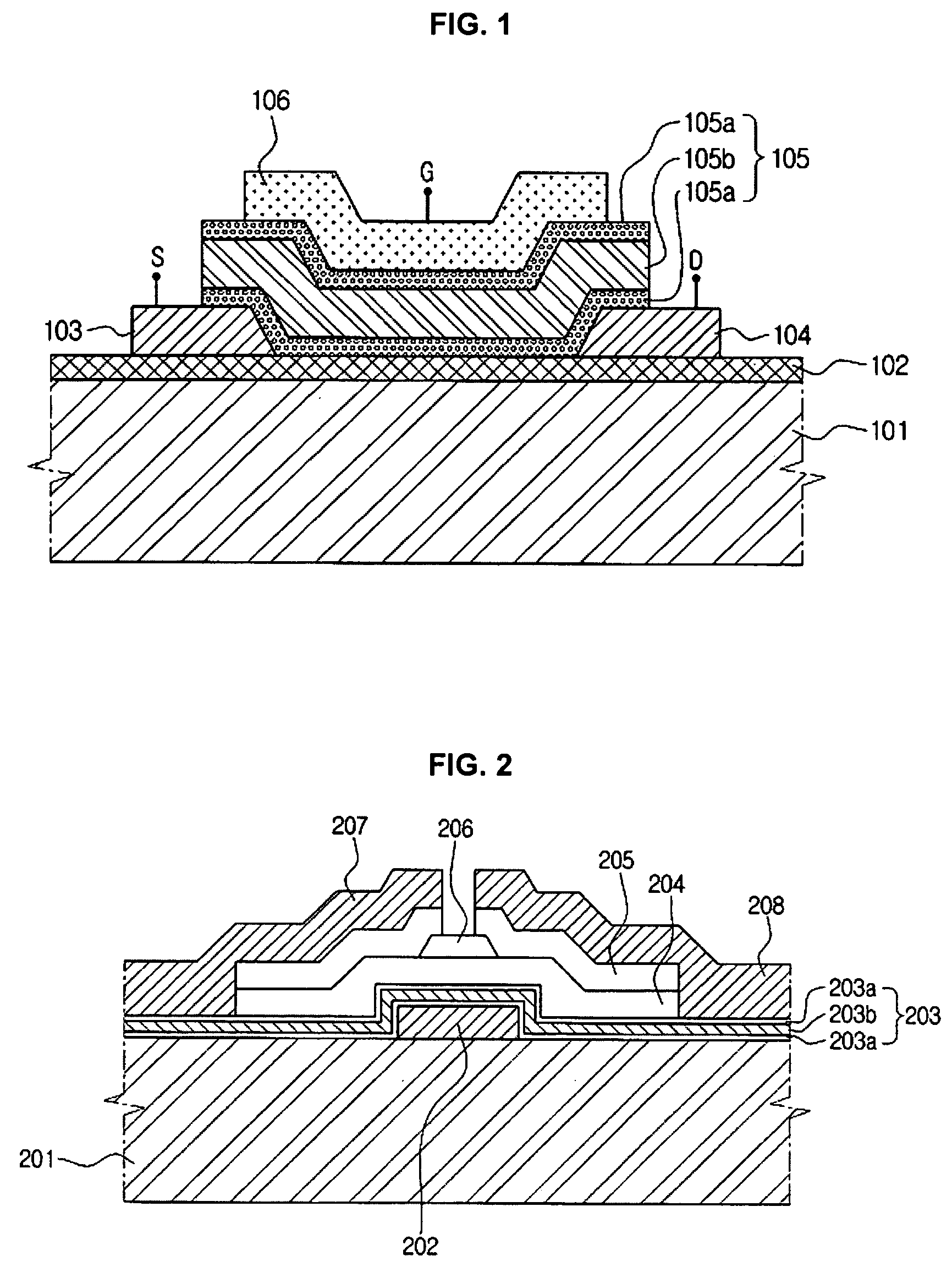
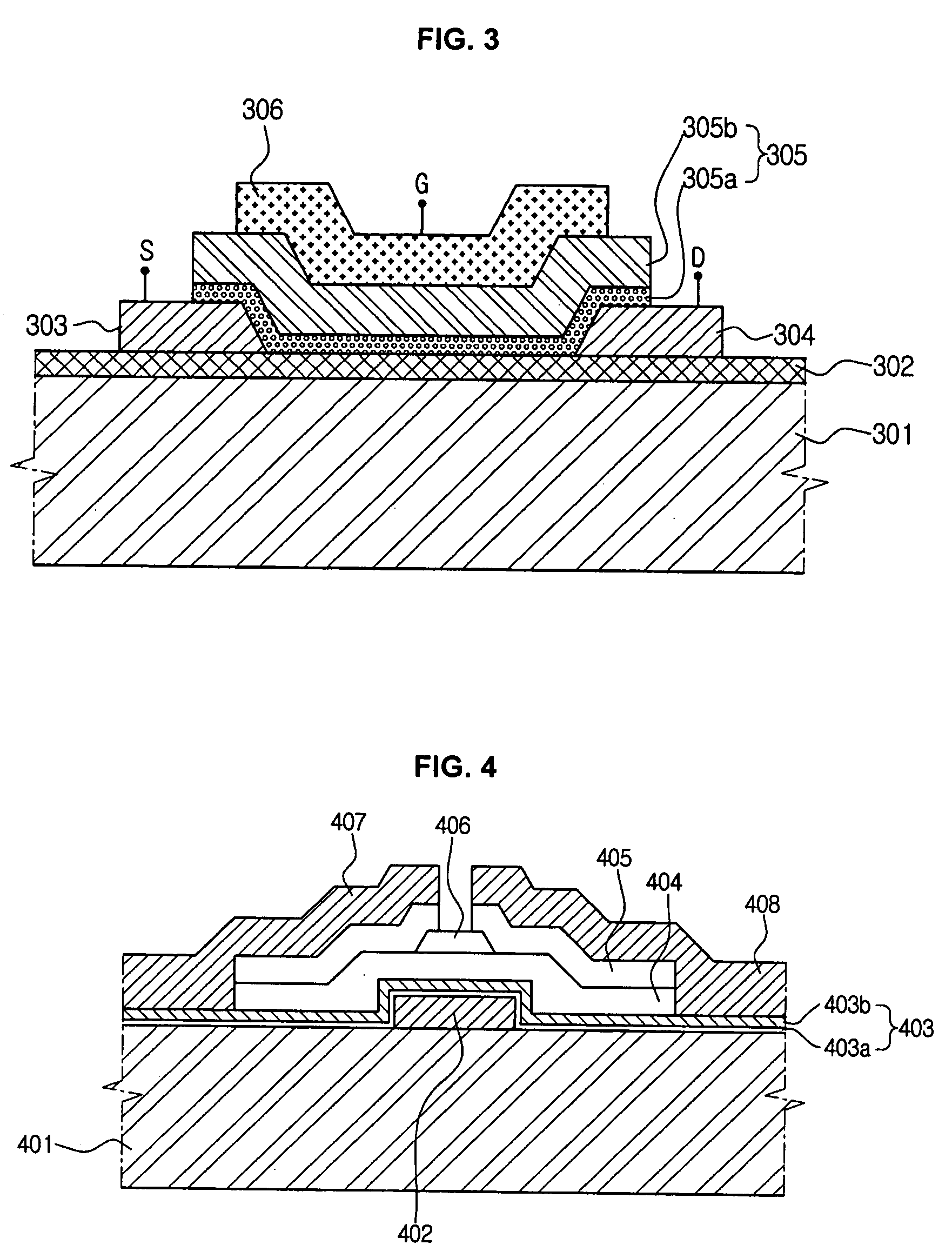
[0031]In example embodiments of a thin film transistor (TFT) according to the present invention, an oxide semiconductor may be used as a channel layer, and a gate insulating layer may include one or more first dielectric layer and a second dielectric layer. Here, the first dielectric layer and the second dielectric layer may have diffe...


PUM


Abstract

There is provided a thin film transistor (TFT) capable of improving electron mobility and minimizing the occurrence of hysteresis due to traps. The TFT includes a channel layer and a gate insulating layer, wherein the channel layer is made of an oxide semiconductor. In the TFT, the gate insulating layer includes one or more first dielectric layer and a second dielectric layer, and the first dielectric layer has a dielectric constant different from that of the second dielectric layer.

Description

PRIORITY STATEMENT[0001]This application claims priority under 35 U.S.C. §119(a) to Republic of Korea Patent Application No. 10-2008-0043329, filed on May 9, 2008 and Republic of Korea Patent Application No. 10-2008-0088905, filed on Sep. 9, 2008, in the Korean Intellectual Property Office (KIPO), the entire contents of which are incorporated herein by reference.BACKGROUND[0002]1. Technical Field[0003]Example embodiments relate to a thin film transistor, and more particularly, to a thin film transistor capable of improving electron mobility and minimizing the occurrence of hysteresis due to traps.[0004]2. Discussion of the Related Art[0005]A flat panel display such as an organic light emitting diode (OLED) or a liquid crystal display (LCD) has a thin film transistor (TFT) as a switching element. The TFT is divided into a top-gate type and a bottom-gate type depending on the position of a gate electrode. However, both the top-gate type and the bottom-gate type TFTs include a channel ...

Claims


Application Information

Patent Timeline
Patent Type & Authority Applications(United States)
IPC IPC(8): H01L29/786
CPCH01L29/4908H01L29/7869
Inventor LEE, SANG YEOLCHANG, SEONGPIL
Owner KOREA INST OF SCI & TECH
Why Eureka
Try Eureka