Quantum-well photoelectric device assembled from nanomembranes

Active Publication Date: 2009-11-19
WISCONSIN ALUMNI RES FOUND
View PDF5 Cites 6 Cited by
  • Summary
  • Abstract
  • Description
  • Claims
  • Application Information

AI Technical Summary

Benefits of technology

[0013]The present invention provides an improved method of manufacturing a quantum cascade laser or similar quantum-well device by the manipulation and assembly of physically separate monocrystalline semiconductor layers. In one embodiment, this technique may be used to produce a superior virtual substrate by detaching a symmetric multilayer structure from its substrate,

Problems solved by technology

Quantum cascade lasers with significant power may require many defect-free layers of semiconductor and barrier material.
Defects are imperfections in the crystal structure that adversely affect movement of electrons or holes through the device.
Despite best efforts, however, s

Method used


Image

  • Quantum-well photoelectric device assembled from nanomembranes
  • Quantum-well photoelectric device assembled from nanomembranes
  • Quantum-well photoelectric device assembled from nanomembranes

Examples


Example

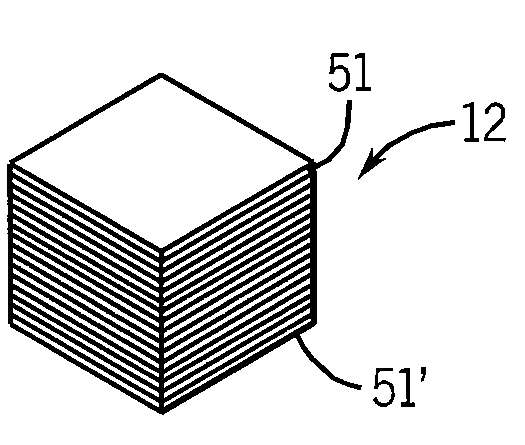
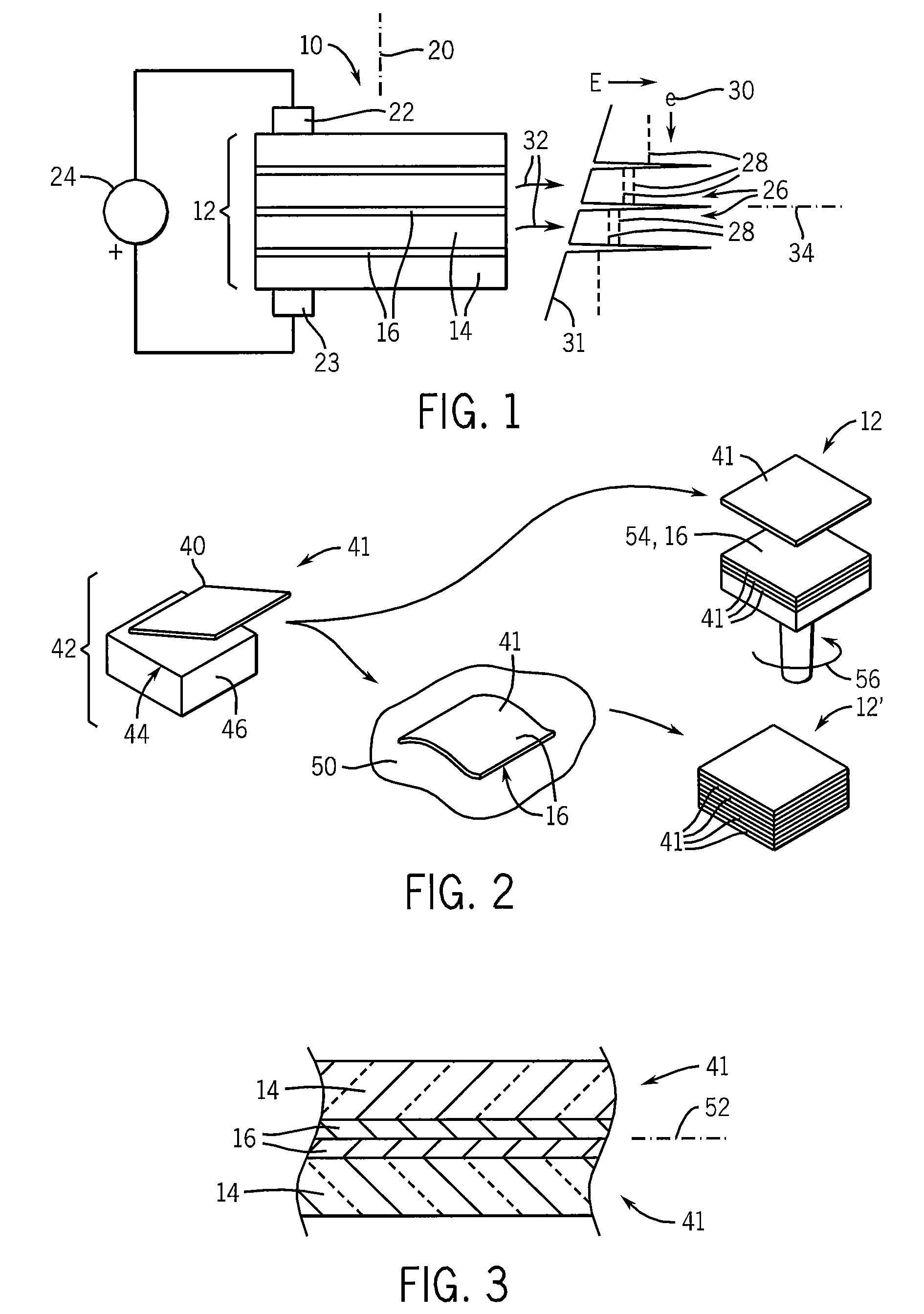
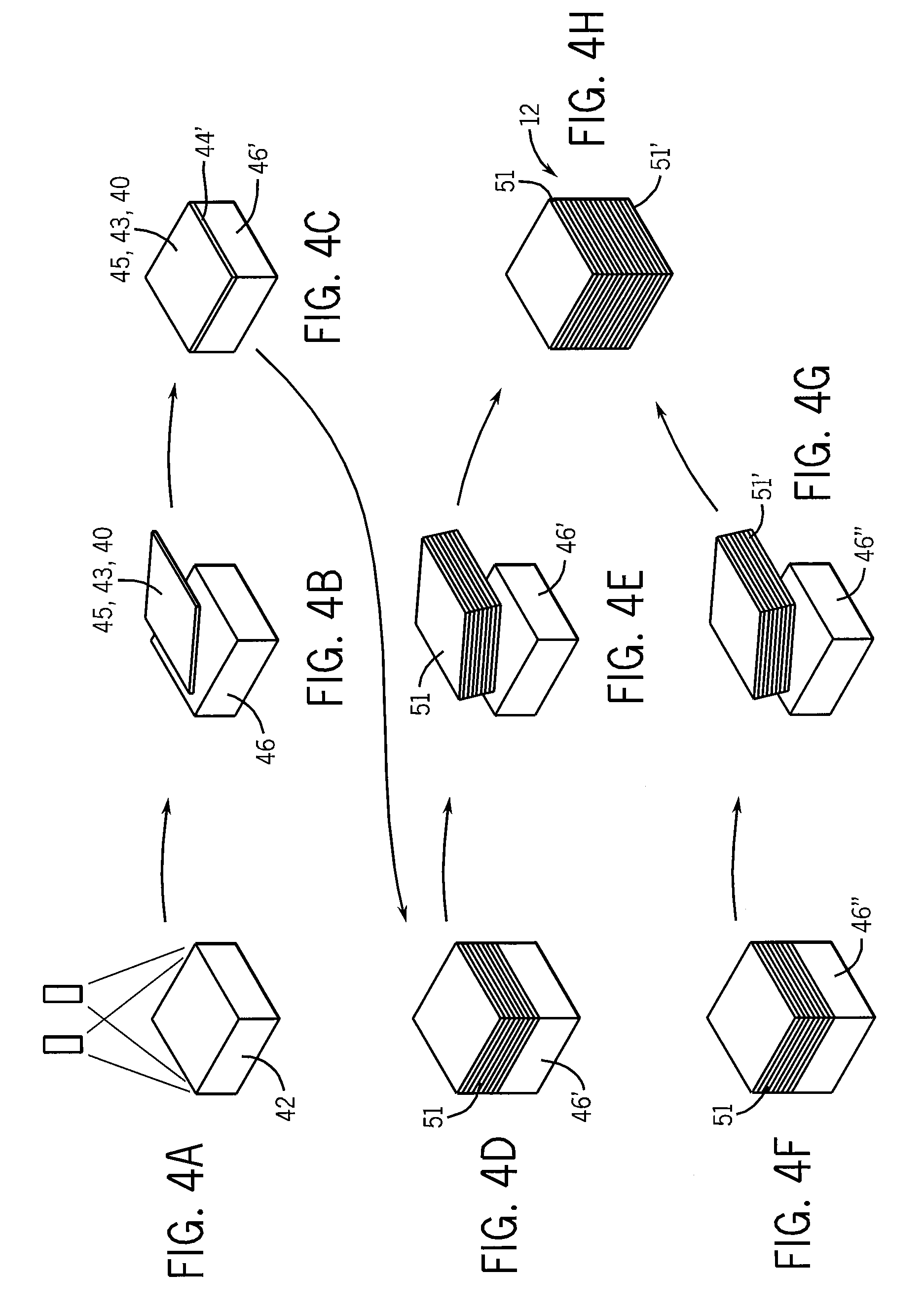
[0046]Referring now to FIG. 1, the present invention provides a quantum-well photoelectric device such as a silicon-based quantum cascade laser 10. The laser 10 employs a stack 12 of semiconductor layers 14 separated by barrier layers 16, preventing classical electron flow. The number of layers shown in FIG. 1 is greatly reduced for clarity.

[0047]The stack 12 extends generally along an axis 20 with each of the layers 14 and 16 generally perpendicular to the axis 20, and the outer layers 14 attached to electrodes 22 and 23 which may be biased with an electrical voltage source 24 to provide, in this example, a negative relative voltage at the top of the stack 12 at electrode 22, providing a source of electrons that are drawn to positive relative voltage at the bottom of the stack 12 at electrode 23.

[0048]The barrier layers 16 surrounding each semiconductor layer 14 provide a high dielectric electrical insulation producing quantum well 26 shown in a potential energy line 31 depicting g...


PUM


Abstract

A quantum-well photoelectric device, such as a quantum cascade laser, is constructed of monocrystalline nanoscale membranes physically removed from a substrate and mechanically assembled into a stack.

Description

STATEMENT REGARDING FEDERALLY SPONSORED RESEARCH OR DEVELOPMENT[0001]This invention was made with United States government support awarded by the following agency:[0002]DOE DE-FG02-03ER46028 NSF 0325634[0003]The United States has certain rights in this invention.CROSS REFERENCE TO RELATED APPLICATION[0004]Not Applicable.BACKGROUND OF THE INVENTION[0005]The present invention relates to solid-state lasers and specifically to a method of fabricating a quantum-well photoelectric device, for example, a quantum cascade laser or quantum cascade photodetector.[0006]Quantum cascade lasers emit light when electrons (holes) cascade through a series of quantum wells positioned between electrodes of the laser. The electrodes create an energy gradient among successive quantum wells, and within a quantum well, transient confinement of electrons (holes) splits the conduction (valence) band of the semiconductor into subbands. When the electrons (holes) pass between the subbands, stimulated emission ...

Claims


Application Information

Patent Timeline
IPC IPC(8): H01L31/00H01L21/02
CPCB82Y20/00H01L31/035254H01S5/3427H01S5/3402H01S5/3407H01S5/021Y10S438/962
Inventor ERIKSSON, MARK A.LAGALLY, MAX G.KIEFER, ARNOLD MELVIN
Owner WISCONSIN ALUMNI RES FOUND
Why Eureka
Try Eureka