Integrated electronics matching circuit at an antenna feed point for establishing wide bandwidth, low vswr operation, and method of design
- Summary
- Abstract
- Description
- Claims
- Application Information
AI Technical Summary
Benefits of technology
Problems solved by technology
Method used
Image
Examples
Embodiment Construction
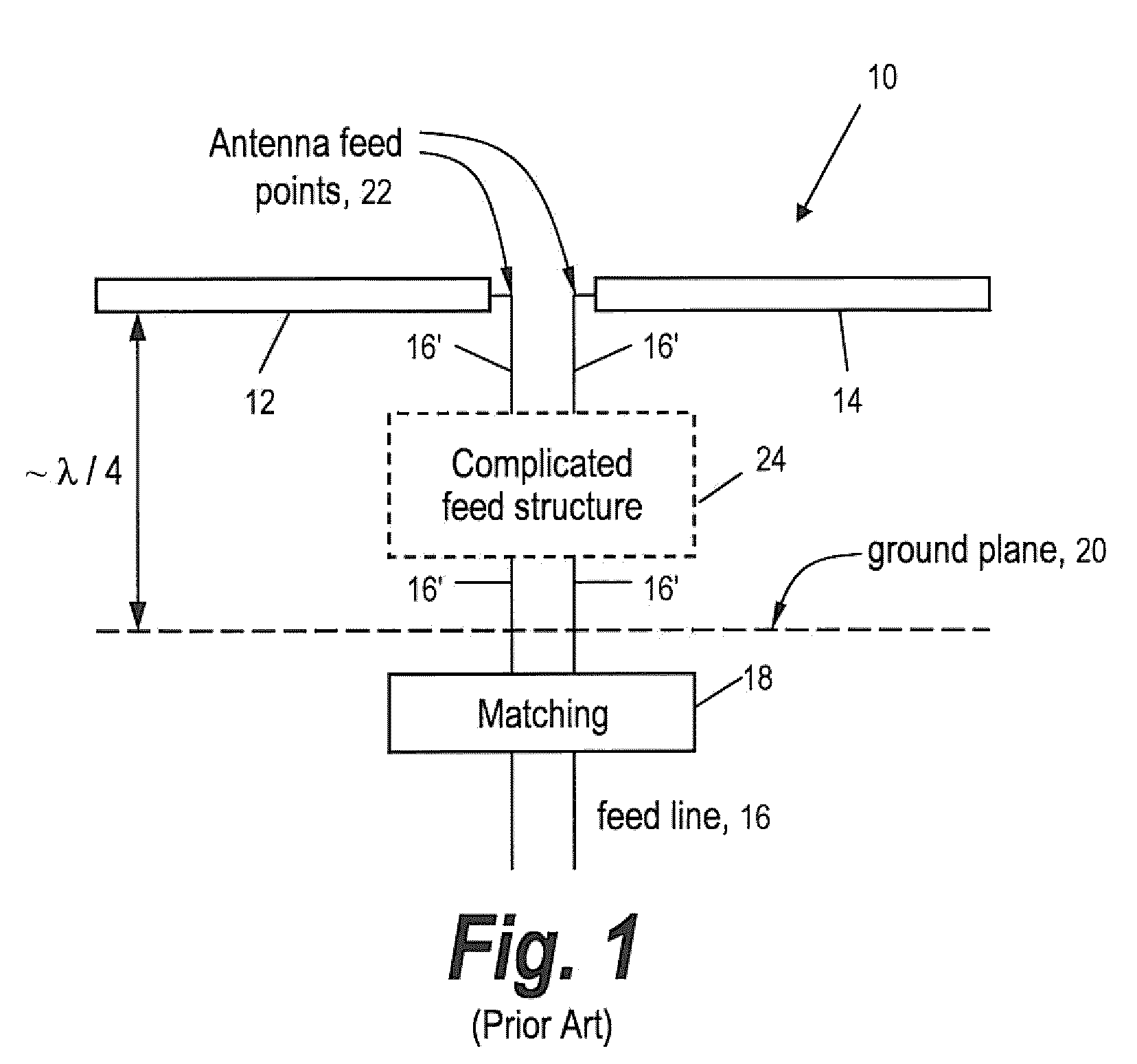
[0047]Referring now to FIG. 1, in the prior art an antenna here pictured as a dipole 10 having dipole elements 12 and 14 is to be connected to a feed line 16, with the feed line to be matched to the antenna. In the past, in order to accomplish this a matching circuit 18 was located below the ground plane 20 for antenna 10. This located the matching circuit oftentimes a quarter of a wavelength away from the antenna feed points 22 of antenna 10.
[0048]In the past, complex impedance interfaces to planar antenna elements placed below the ground plane involved long connection lines to the antenna feed point and used non-ideal components. These long connection lines, here illustrated at 16′, introduce parasatics and artifacts which in turn restrict antenna bandwidth.
[0049]As mentioned above, it is important to have an efficient coupling system for the antenna feed point to the transmission line to minimize VSWR problems and to be able to provide a wide bandwidth for the antenna. When the e...
PUM
 Abstract
Description
Claims
Application Information


