
Eureka
For R&D, Eureka makes reading and utilizing patents & technical documents easy.
Eureka AIR
Designed for self-driven R&D workflows. Generate viable solutions, solve complex R&D challenges, empower your innovation with AI.

Eureka Materials
Designed for material experts only. Revolutionize your material R&D, from search, analyze, to developing new materials.

TechResearch
Generate reliable direction feasibility study reports for your R&D in just a few steps.

TechSeek
Discover and master advanced knowledge NOW. Basics, ideas, possibilities, all at once.

TechMind
As an expert in R&D Theories, TechMind can generates customized viable solutions instantly.

TechRisk
Analyze your overall solution with one click, know your potential R&D risks in advance.

TechMonitor
Get weekly tech updates, stay abreast of the latest tech innovations and key insights.
Semiconductor device pattern verification method, semiconductor device pattern verification program, and semiconductor device manufacturing method
- Summary
- Abstract
- Description
- Claims
- Application Information
AI Technical Summary
Benefits of technology
Problems solved by technology
Method used
Image

Examples
first embodiment
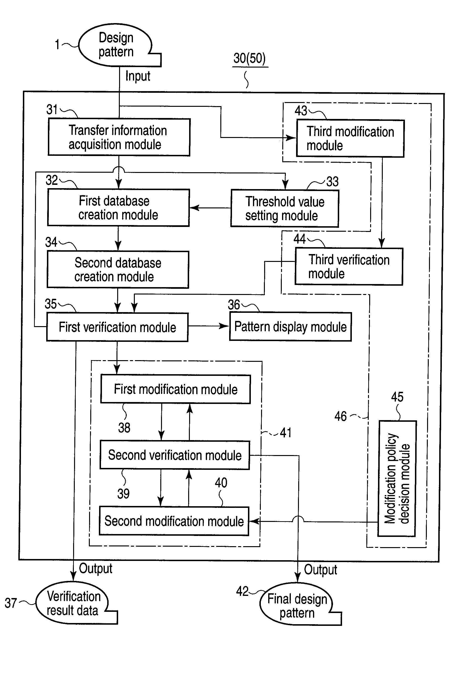
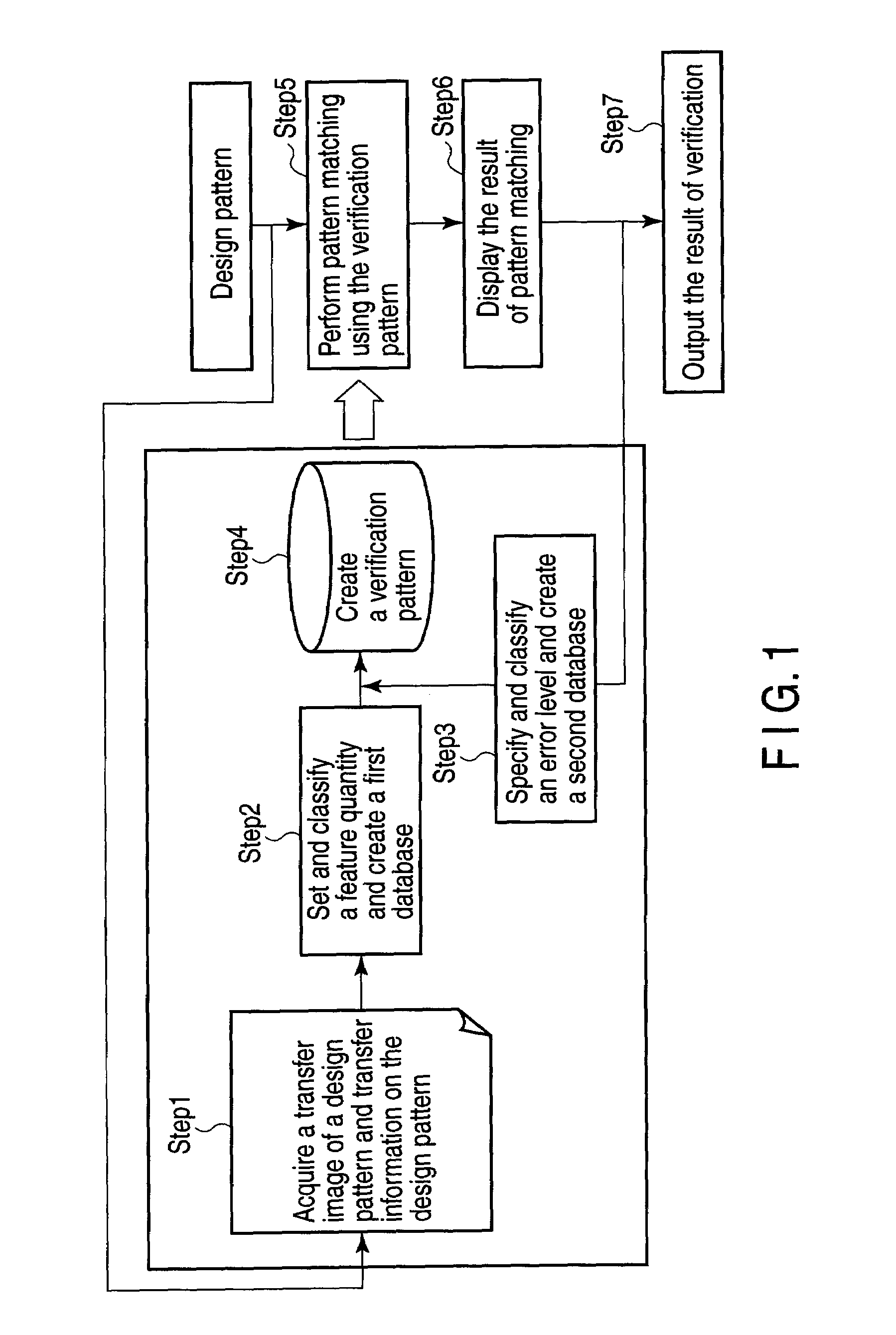
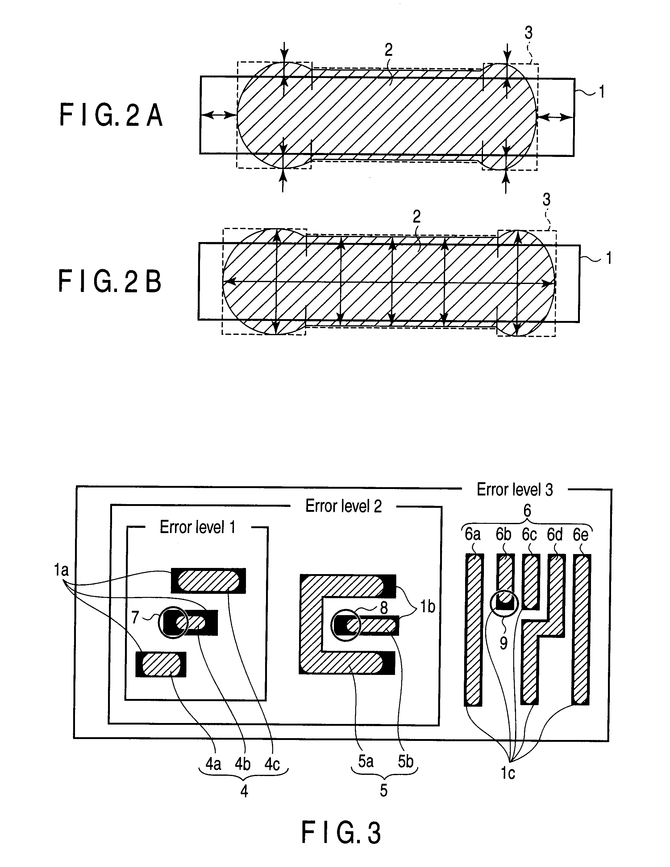
[0027]A first embodiment of the invention relates to a design pattern verification method, a design pattern verification system, and a design pattern verification program which are applied in creating a physical layout of a semiconductor integrated circuit pattern from design data on a semiconductor integrated circuit pattern. In the first embodiment, an explanation will be given as to a pattern verification method, a pattern verification system, and a pattern verification program which perform verification of the process margin of the pattern on a substrate concurrently with the creation of design data on a semiconductor integrated circuit pattern. In the first embodiment, the verification of the process margin of a pattern is virtual pattern matching. To perform verification concurrently during pattern design, it is necessary to process the spots to be verified at high speed with high accuracy. To do this, it is desirable to quickly extract data on a pattern to be verified from da...
second embodiment
[0084]Next, a second embodiment of the invention will be explained. In the second embodiment, the same parts as those of the first embodiment are indicated by the same reference numeral and a detailed explanation of them will be omitted.
[0085]The second embodiment relates to a pattern design method, a pattern design system, and a pattern design program which make use of the pattern verification method, pattern verification system, and pattern verification program of the first embodiment, respectively. Specifically, in the second embodiment, a pattern design method, a pattern design system, and a pattern design program will be explained which, when design data on a semiconductor integrated circuit pattern is created, verify a process margin concurrently with pattern design and modify a design pattern whose process margin has not reached an allowable error margin by the time the chip design has been completed. In the second embodiment, the layout of the individual functional blocks of...
third embodiment
[0142]Next, a third embodiment of the invention will be explained mainly with reference to FIG. 20. In the third embodiment, the same parts as those of the first and embodiments are indicated by the same reference numerals and a detailed explanation of them will be omitted.
[0143]The third embodiment relates to a pattern design method, a pattern design system, and a pattern design program which make use of the pattern verification method, pattern verification system, and pattern verification program of the first embodiment and the pattern design method, pattern design system, and pattern design program of the second embodiment, respectively. The third embodiment differs greatly from the first and second embodiments in that the third embodiment includes the process of changing the layout of a pattern before verifying a design pattern, taking into account information on defects in the pattern.
[0144](Pattern Design Method)
[0145]Hereinafter, a pattern design method according to the third...
PUM
 Abstract
Description
Claims
Application Information
 - R&D Engineer
- R&D Manager
- IP Professional
- Industry Leading Data Capabilities
- Powerful AI technology
- Patent DNA Extraction
Browse by: Latest US Patents, China's latest patents, Technical Efficacy Thesaurus, Application Domain, Technology Topic, Popular Technical Reports.
© 2024 PatSnap. All rights reserved.Legal|Privacy policy|Modern Slavery Act Transparency Statement|Sitemap|About US| Contact US: help@patsnap.com