Method for Capping a MEMS Wafer

Active Publication Date: 2009-12-03
ANALOG DEVICES INC
View PDF6 Cites 45 Cited by
  • Summary
  • Abstract
  • Description
  • Claims
  • Application Information

AI Technical Summary

Benefits of technology

[0006]In embodiments of the present invention, a method is provided for bonding a cap wafer to a MEMS wafer, which includes a microstructure, to form a hermetic seal. A glass bonding agent is applied to surfaces of the cap wafer which will contact the MEMS wafer. Organic material in the bonding agent is then burned off by heating the cap wafer. The cap wafer/bonding agent combination is then cleaned to remove lead impurities, such as by using oxygen plasma or another cleaning method. The cap wafer is then aligned with and brought into contact with the MEMS wafer with the glass bonding agent forming a contact region between the two wafers. The cap wafer/MEMS wafer combination is then heated

Problems solved by technology

The mechanical structures of the MEMS are typically very fragile, and can be easily damaged.
Furthermore, the mechanical structures of the MEMS are typically very sensitive, and can be easily impeded.
Stiction, which is

Method used


Image

  • Method for Capping a MEMS Wafer
  • Method for Capping a MEMS Wafer
  • Method for Capping a MEMS Wafer

Examples


Embodiment Construction

[0012]Definitions: As used in this description and the accompanying claims, unless the context otherwise requires, a “percentage of a gas” in a gas mixture shall mean the ratio of the number of molecules of the given gas in a volume to the total number of gas molecules in the volume, multiplied by 100 percent.

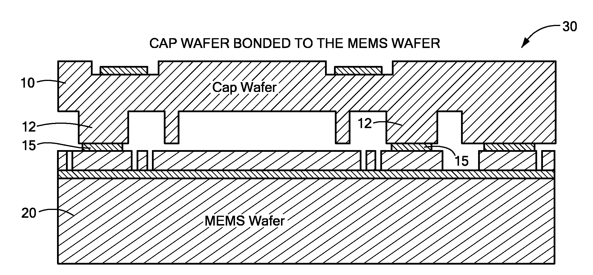
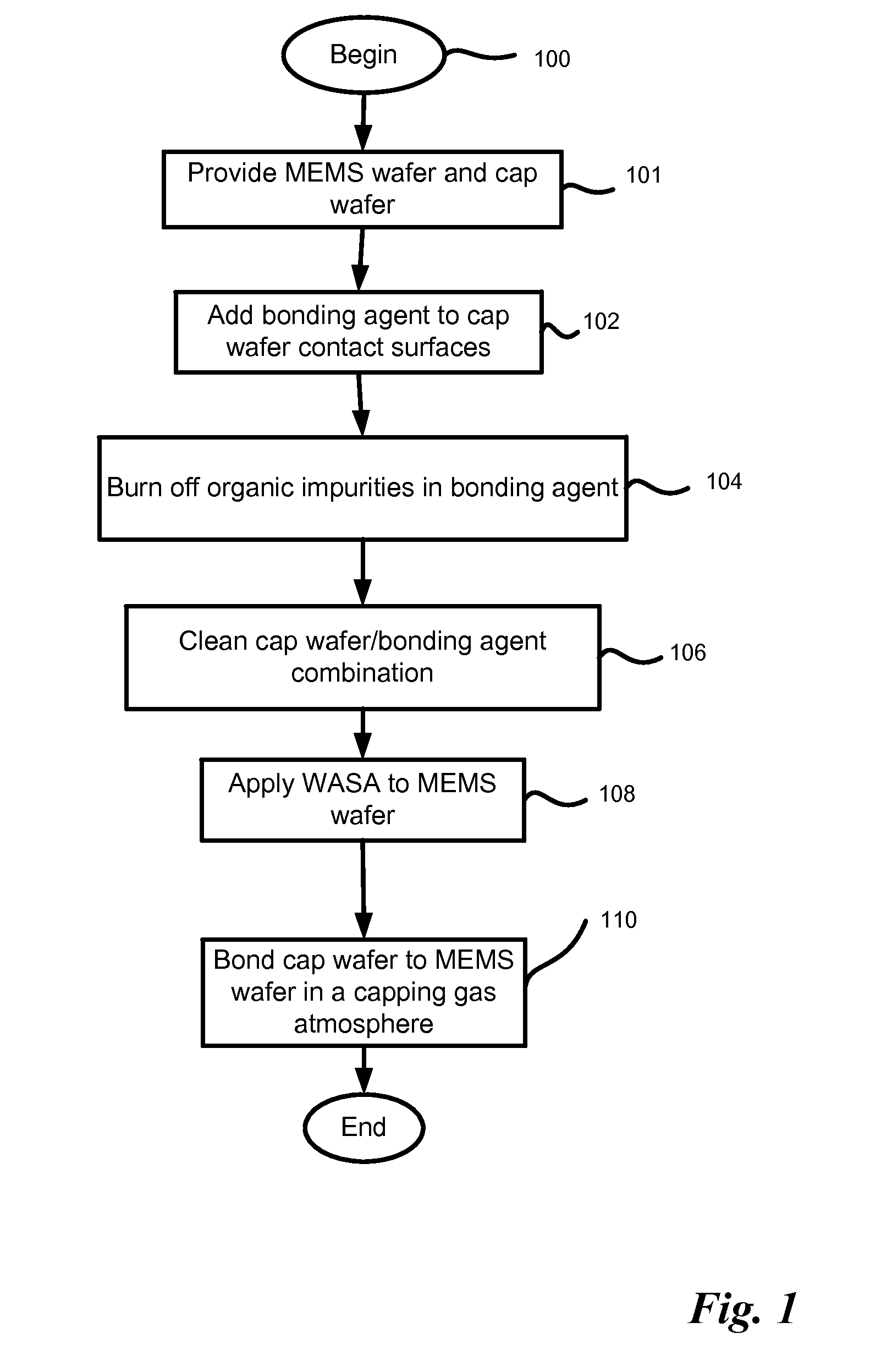
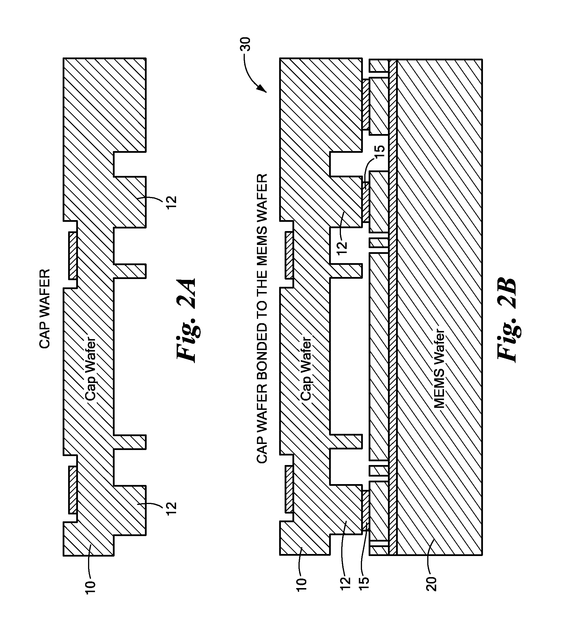
[0013]In embodiments of the present invention, a process is provided for capping a MEMS wafer such that stiction in MEMS device structures is reduced. A glass bonding agent is added to a cap wafer on cap wafer surfaces that will contact the MEMS wafer. After the organic impurities in the bonding material are burned off, the cap wafer / bonding agent is subjected to a further cleaning process to remove other impurities in the bonding material, such as lead. For example, the cap wafer / bonding agent may be cleaned with an oxygen plasma. A WASA is used to coat the MEMS structures and the cleaned cap wafer / bonding agent combination is then bonded to the MEMS wafer in a substantially o...


PUM

PropertyMeasurementUnit
Fractionaaaaaaaaaa
Timeaaaaaaaaaa
Angleaaaaaaaaaa

Abstract

A method for capping a MEMS wafer to form a hermetically sealed device. The method includes applying a glass bonding agent to the cap wafer and burning off organic material in the glass bonding agent. The cap wafer/glass bonding agent combination is then cleaned to reduce lead in the combination. The cleaning is preferably accomplished using an oxygen plasma. The MEMS device is coated with a WASA agent. The cap wafer is then bonded to the MEMS wafer by heating this combination in a capping gas atmosphere of hydrogen molecules in a gas such as nitrogen, argon or neon. This method of capping the MEMS wafer can reduce stiction in the MEMS device.

Description

[0001]This application claims priority from U.S. provisional patent application Ser. No. 61 / 057,261, filed May 30, 2008, attorney docket no. 2550 / C05, which is incorporated herein by reference.TECHNICAL FIELD[0002]The present invention relates to methods for forming hermetically sealed packages for microelectromechanical system (“MEMS”) devices, and more particularly to sealing methods that reduce stiction in MEMS devices.BACKGROUND OF THE INVENTION[0003]Generally speaking, a microelectromechanical system (“MEMS”) is a highly miniaturized device having both electrical and mechanical components. MEMS devices are typically fabricated on or from a substrate material, such as silicon or polysilicon. Various electrical and mechanical structures are formed in the MEMS using a variety of techniques.[0004]The mechanical structures of the MEMS are typically very fragile, and can be easily damaged. Furthermore, the mechanical structures of the MEMS are typically very sensitive, and can be eas...

Claims


Application Information

Patent Timeline
IPC IPC(8): H01L29/84H01L21/50
CPCB81C1/00269B81C1/00293B81C2203/0109H01L23/10H01L2924/0002H01L2924/00
Inventor BHAGAVAT, MILINDTARVIN, ERIKSAMMOURA, FIRASYANG, KUANGSPARKS, ANDREW
Owner ANALOG DEVICES INC
Why Eureka
Try Eureka