
Switching device and testing apparatus

Inactive Publication Date: 2009-12-10
ADVANTEST CORP
View PDF2 Cites 6 Cited by
  • Summary
  • Abstract
  • Description
  • Claims
  • Application Information

AI Technical Summary

Benefits of technology

[0017]Therefore, it is an object of an aspect of the innovations herein to provide a switching device and a testing apparatus which are capable of overcoming the above drawbacks accompanying the related

Problems solved by technology

Therefore, the metal contact deteriorates due to friction and the like.
Furthermore, the mechanical relay cannot be integrated into a semiconductor integrated circuit, which results in a large size and undermines efforts to increase the device density.
Therefore, the photo MOSFET relay is complex in structure, large and expensive.
In addition, the photo MOSFET relay exhibits poor high-frequency characteristics because of the parasitic inductances of the lead frame, bonding wires and the like and the RC product of the on resistance and the gate capacitance of the MOSFET.
Furthermore, since the photocell and the light emitting diode are formed by using a GaAs semiconductor or the like, the photo MOSFET relay cannot be integrated together with other circuits that are formed by using a silicon semiconductor.
For the reasons stated above, the photo MOSFET relay hampers attempts to reduce the size of a device including the photo MOSFET relay, to increase the density of the device and to lower the cost of the device.
The semiconductor relay thus cannot be easily turned on / off.
Furthermore, the switches that are utilized as the I / O relay and the DC relay in the testing apparatus desirably have a long lifetime.

Method used


Image

  • Switching device and testing apparatus
  • Switching device and testing apparatus
  • Switching device and testing apparatus

Examples


Embodiment Construction

[0031]Some aspects of the invention will now be described based on the embodiments, which do not intend to limit the scope of the present invention, but exemplify the invention. All of the features and the combinations thereof described in the embodiment are not necessarily essential to the invention.

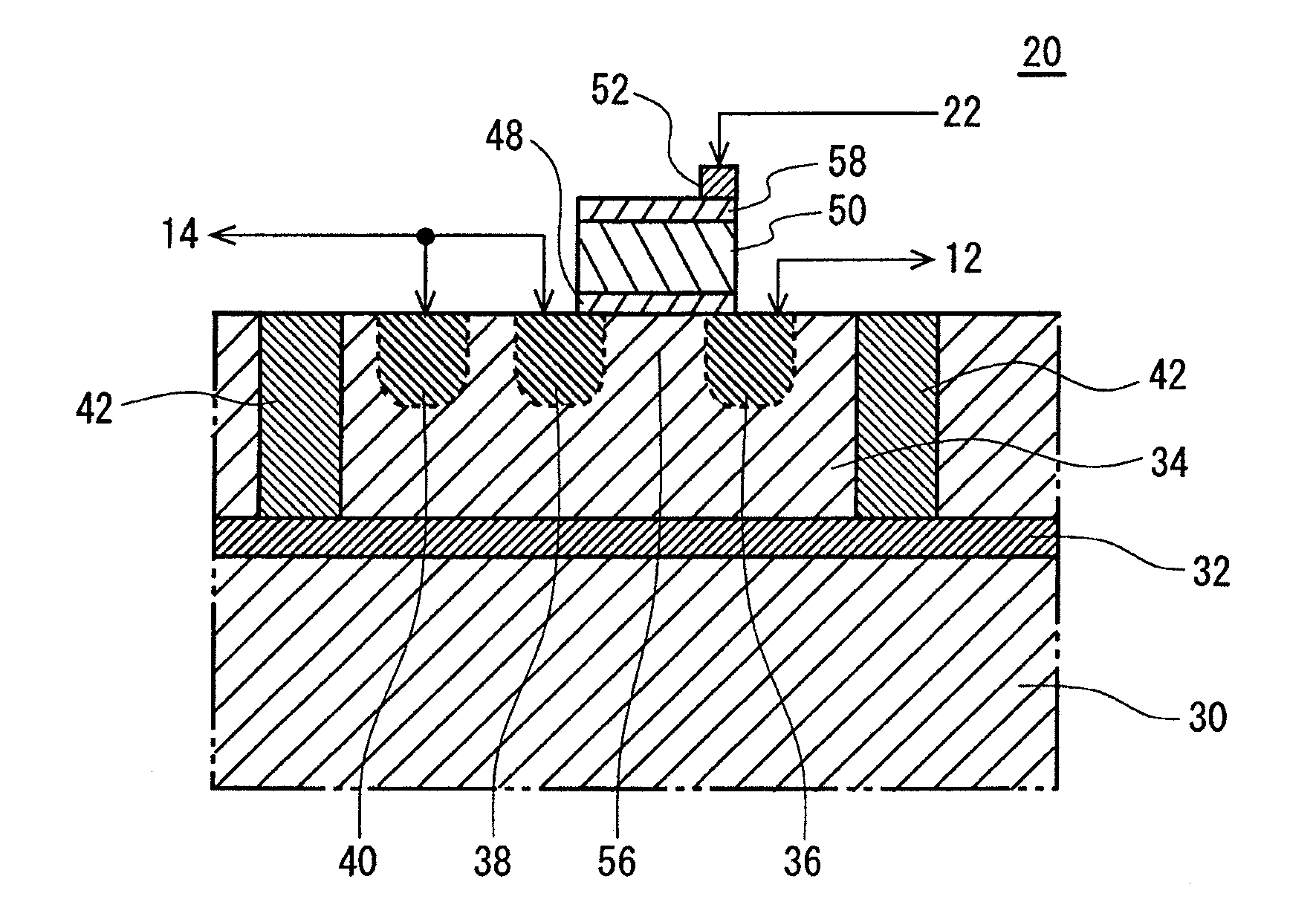
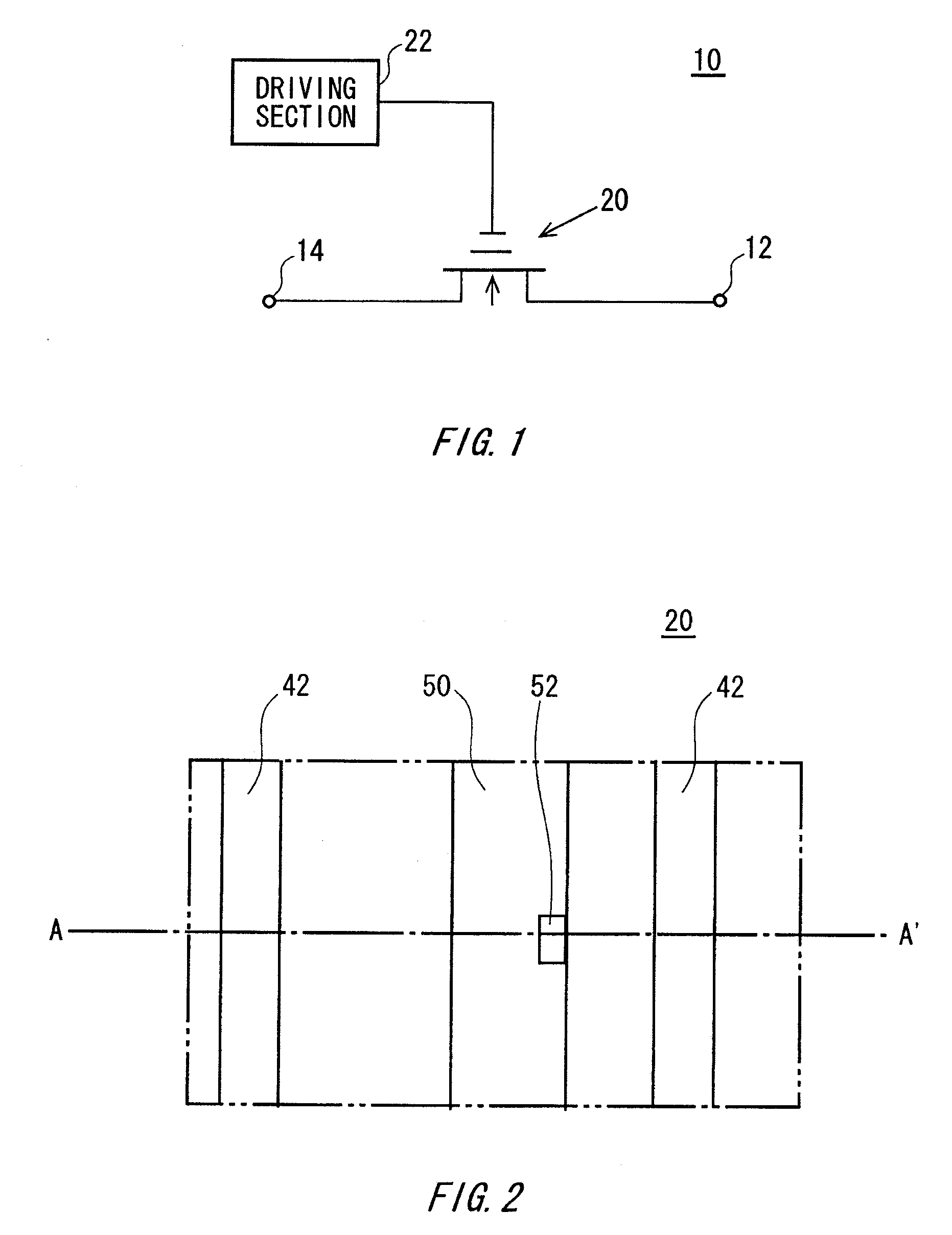
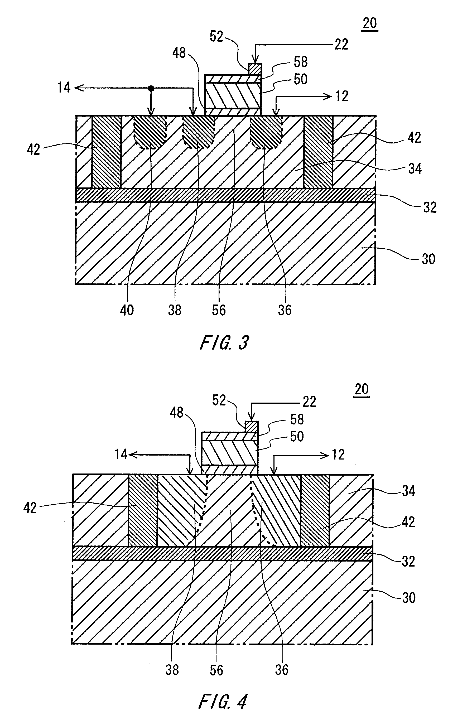
[0032]FIG. 1 illustrates the configuration of a switching device 10 relating to an embodiment of the present invention. The switching device 10 includes a semiconductor switch 20 and a driving section 22. The switching device 10 electrically connects or disconnects a first terminal 12 and a second terminal 14 to / from each other. The semiconductor switch 20 is formed on a semiconductor, and electrically connects or disconnects its drain and its source to / from each other (i.e., turned on or off) depending on a driving voltage supplied to its gate. The semiconductor switch 20 may be of an n-channel type whose majority carrier of the current flowing between the drain and the source is elect...


PUM


Abstract

There is provided a switching device that electrically connects or disconnects a first terminal and a second terminal to / from each other. The switching device includes a semiconductor layer, a drain electrode that is formed in the semiconductor layer, where the drain electrode is connected to the first terminal, a source electrode that is formed in the semiconductor layer, where the source electrode is connected to the second terminal, a gate insulator that is formed on the semiconductor layer between the drain electrode and the source electrode, a floating gate that is formed on the gate insulator, where the floating gate retains a charge therein, and a tunnel gate that is formed on the floating gate, the tunnel gate supplying a tunnel current determined by a driving voltage applied thereto to charge or discharge the floating gate.

Description

CROSS REFERENCE TO RELATED APPLICATION[0001]This is a continuation application of PCT / JP2007 / 066267 filed on Aug. 22, 2007 which claims priority from a Japanese Patent Application NO. 2006-253846 filed on Sep. 20, 2006, the contents of which are incorporated herein by reference.BACKGROUND[0002]1. Technical Field[0003]The present invention relates to a switching device and a testing apparatus. More particularly, the present invention relates to a switching device that connects or disconnects, to / from each other, a drain electrode and a source electrode provided on a semiconductor layer and to a testing apparatus using the same.[0004]2. Related Art[0005]Patent Document 1 discloses a mechanical relay using a reed switch surrounded by a metal guard pipe. The mechanical relay achieves excellent high-frequency characteristics since the guard pipe and the reed switch are arranged coaxially. Patent Document 2 discloses an photo MOSFET relay. The photo MOSFET relay is a semiconductor relay a...

Claims


Application Information

Patent Timeline
IPC IPC(8): H01L29/788H01L23/58G01R31/02
CPCG01R31/2621G01R31/319H01L21/28273H01L21/84H01L27/11519H01L27/11521H01L27/1203H01L2924/0002H01L29/42328H01L29/42332H01L29/7883H01L29/7887H01L2924/00H01L29/40114H10B41/10H10B41/30H01L27/04H01L29/788G01R31/28
Inventor OKAYASU, TOSHIYUKI
Owner ADVANTEST CORP
Learn More