Package on Package Structure with thin film Interposing Layer

a technology of interposing layer and package structure, which is applied in the direction of semiconductor devices, semiconductor/solid-state device details, electrical devices, etc., can solve the problems of reducing the footprint of each, the current state of the art, and the inability to increase density while reducing area, so as to reduce the footprint of each package and reduce the thickness of the interposing layer, the effect of increasing versatility in assembly component selection

Inactive Publication Date: 2009-12-17
TEXAS INSTR INC
View PDF4 Cites 2 Cited by
  • Summary
  • Abstract
  • Description
  • Claims
  • Application Information

AI Technical Summary

Benefits of technology

[0006]In carrying out the principles of the present invention, in accordance with preferred embodiments thereof, the invention provides novel and useful improvements for vertically stacked semiconductor device assemblies. Through diligent study, experimentation, and analysis, the inventor has determined that thin film interposing layers may be used in order to overcome some of the problems with traditional rigid interposing layers known in the arts. Endeavors to use thin film interposers for vertically coupling layers of semiconductor stack assemblies, in order to reduce the thickness of the assemblies, have led to synergistic innovations in using thin film based interposers to realize further advantages such as increased electrical connection density, improved layout flexibility, reduced manufacturing costs, and in some cases increased mechanical strength and durability. Using the invention, the interposing layer may be provided with a full array of fine pitch of electrical contact pads. Advantages also accrue when contact pads are called for on the periphery only, as they may be provided at a higher density than previously known in the art. Aspects of the invention are directed to making vertical interconnections among layers in a stack assembly without the need for using potentially more complex and expensive through-silicon via technology, increasing design flexibility and reducing manufacturing costs.
[0013]The invention has advantages including but not limited to one or more of the following: decreased footprint in package on package structures; decreased interposing layer thickness; increased versatility in assembly component selection; improved interlayer connections; reduced warpage; and reduced cost. These and other features, advantages, and benefits of the present invention can be understood by one of ordinary skill in the arts upon careful consideration of the detailed description of representative embodiments of the invention in connection with the accompanying drawings.

Problems solved by technology

Efforts are continuously being made to design and manufacture devices and packages with reduced area, but attempts to increase density while reducing area eventually reach a practical limit.
Problems remain in the present state of the art, however.
The desirability of reducing the footprint of the assembly, and thus the footprint of each respective layer, is beset with challenges including pitch and layout limitations inherent in forming the interposing layer using a rigid substrate material.
The expense of fashioning such an interposing layer is prohibitive in some instances, particularly in applications where fine pitch microbump interconnections are desired.
In applications where interlayer vertical connections are desired, efforts to use through-silicon vias in the interposing layer substrate are beset with manufacturing difficulties that rapidly increase the expense of manufacturing as the available area decreases.
Unfortunately, with the substrate materials used in the arts, a certain minimum thickness is required in order to provide the interposing layer with sufficient mechanical strength to withstand manufacturing and handling operations, and to resist warping.
Warping of the overall assembly can be an additional problem, particularly in cases where stack layers of varying areas are used, resulting in overhangs susceptible to warpage.
Other considerations, which can lead to further complications, include the need to keep electrical connections short to optimize speed, and to provide design flexibility for addressing layout and timing concerns.

Method used


Image

  • Package on Package Structure with thin film Interposing Layer
  • Package on Package Structure with thin film Interposing Layer
  • Package on Package Structure with thin film Interposing Layer

Examples


Embodiment Construction

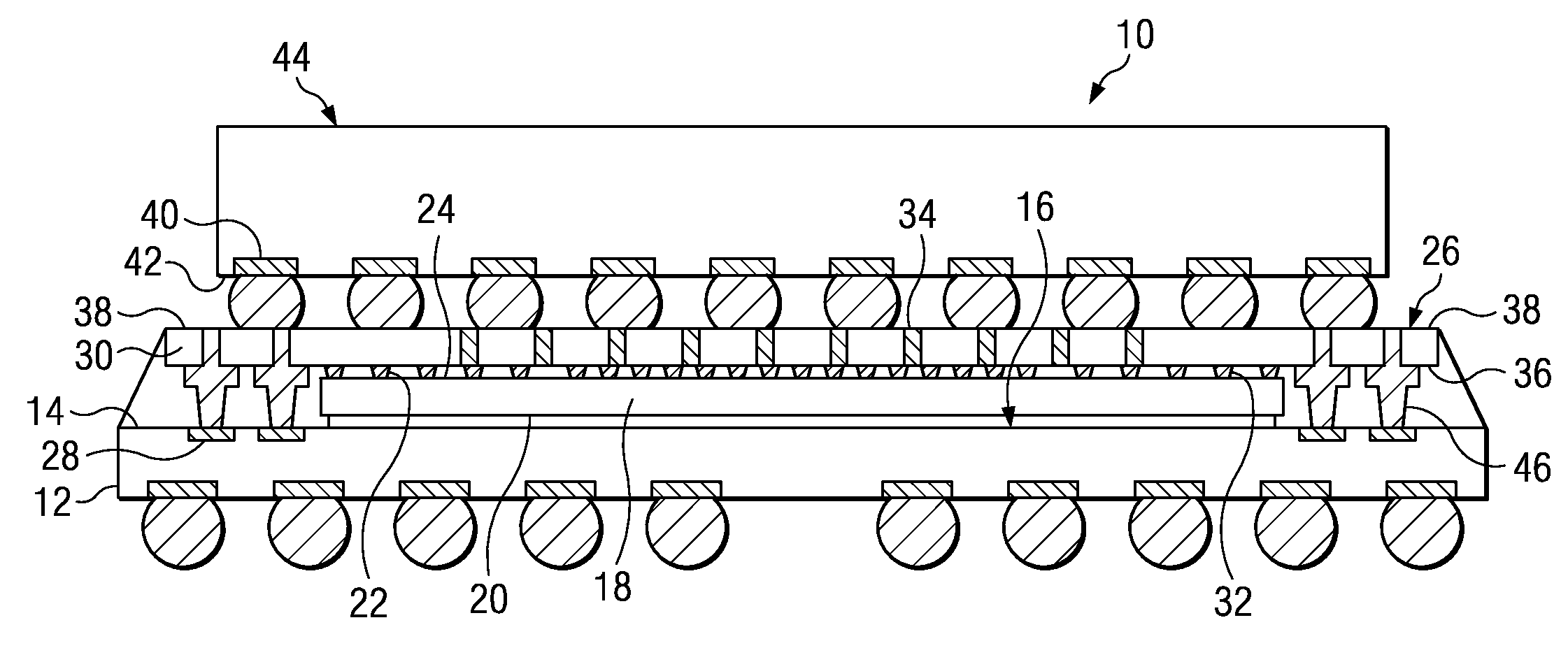
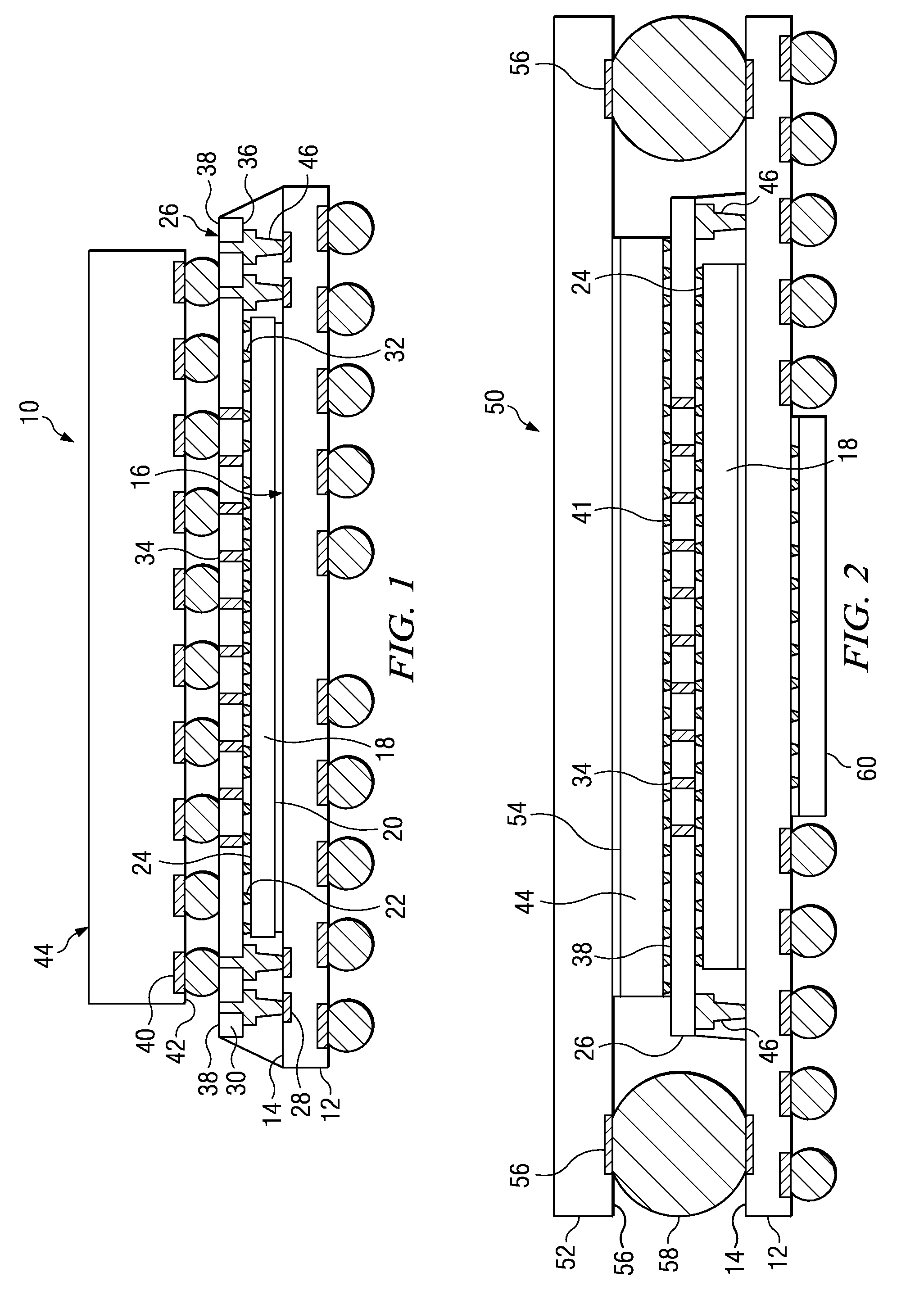
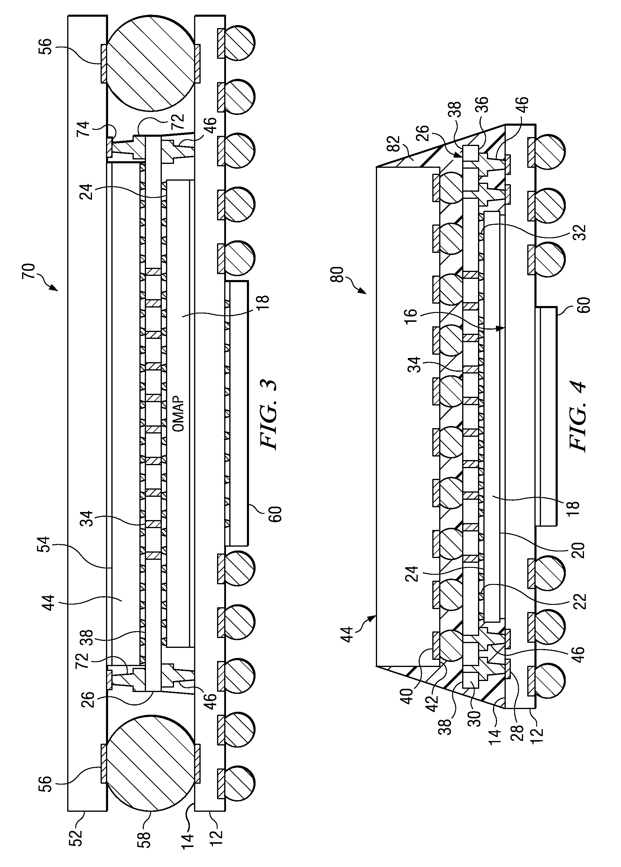
[0020]While the making and using of various exemplary embodiments of the invention are discussed herein, it should be appreciated that the present invention provides inventive concepts which can be embodied in a wide variety of specific contexts. It should be understood that the invention may be practiced with vertically stacked semiconductor package on package assemblies and associated manufacturing processes of various types and materials without altering the principles of the invention. For purposes of clarity, detailed descriptions of functions and systems familiar to those skilled in the semiconductor device, packaging, and manufacturing arts are not included.

[0021]In general, the invention provides vertically stacked semiconductor device assemblies using thin film or tape interposing layers structured for vertically coupling layers of the stack. Features of the invention are advantageous in terms of increased electrical connection density, decreased assembly footprint, decreas...


PUM


Abstract

The invention relates to microelectronic semiconductor device assemblies having vertically stacked semiconductor device layers. In a disclosed example of a preferred embodiment, a semiconductor device includes a base substrate, an interposing layer, and a second semiconductor device. The interposing layer features a thin insulating film with numerous electrical contacts on its surfaces for electrically coupling with electrical contacts on the adjacent layers. The interposing layer further includes electrical contacts for coupling with one or more non-adjacent layers. Particular examples of preferred embodiments of the invention disclose the use of polyimide film for the interposing layer material and metal studs for non-adjacent layer contacts.

Description

TECHNICAL FIELD[0001]The invention relates to electronic semiconductor chips and manufacturing. More particularly, the invention relates to systems and associated methods for manufacturing vertically stacked semiconductor device assemblies with improved interposing layers between semiconductor device layers.BACKGROUND OF THE INVENTION[0002]There is generally an ongoing need to minimize the size of electronic apparatus. At the same time, the demand for increased features results in an increase in the number of components on a given device. Efforts are continuously being made to design and manufacture devices and packages with reduced area, but attempts to increase density while reducing area eventually reach a practical limit. As designers attempt to maximize the use of substrate, semiconductor device, and system area, vertical stacking of system components becomes increasingly attractive.[0003]In order to reduce or eliminate some of the problems associated with wirebonding and to re...

Claims


Application Information

Patent Timeline
Patent Type & Authority Applications(United States)
IPC IPC(8): H01L23/538
CPCH01L23/49811H01L23/49816H01L2225/1058H01L2225/1023H01L2924/3511H01L2924/18161H01L2224/32225H01L2224/32145H01L2224/16225H01L2924/0001H01L2224/13147H01L23/49827H01L23/5389H01L24/16H01L24/32H01L24/73H01L25/105H01L2224/16235H01L2224/73204H01L2224/73253H01L2924/01029H01L2924/01079H01L2924/01082H01L2924/15311H01L2924/1532H01L2924/15321H01L2224/131H01L2924/01033H01L2924/00012H01L2924/00H01L2924/00014H01L2924/014H01L2224/13099H01L2224/05571H01L2224/05573H01L2224/05599
Inventor GERBER, MARK ALLEN
Owner TEXAS INSTR INC
Why Eureka
Try Eureka