

Organic light emitting display and its method of fabrication
- Summary
- Abstract
- Description
- Claims
- Application Information
AI Technical Summary
Benefits of technology
Problems solved by technology
Method used
Image

Examples
first embodiment
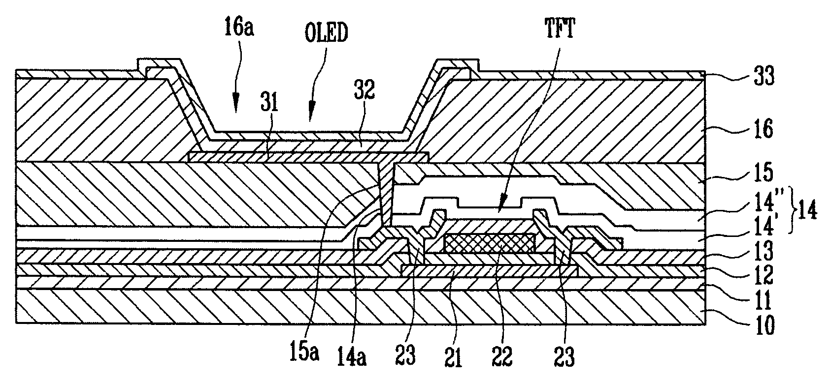
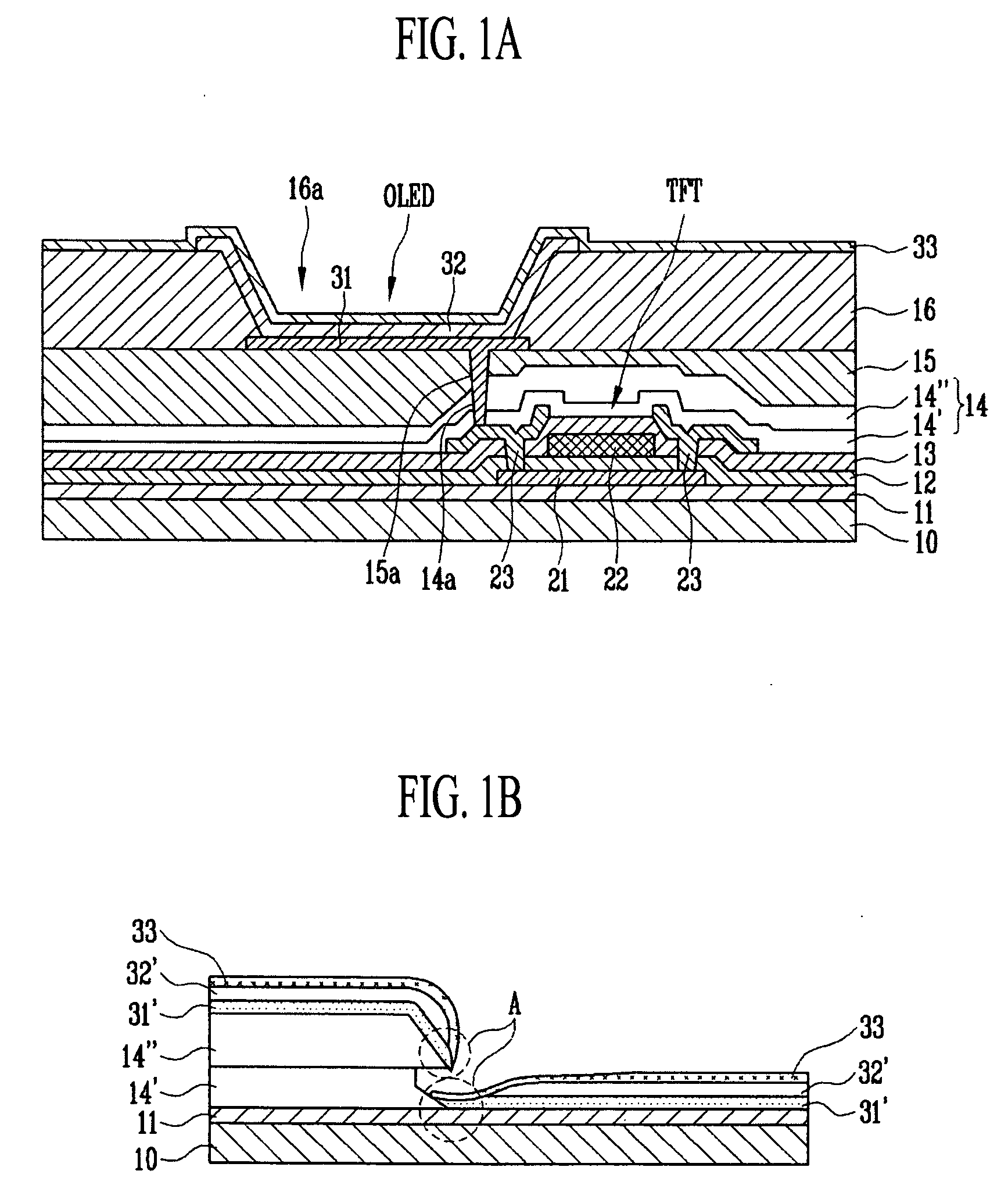
[0031]FIGS. 1A and 1B are cross-sectional views of an organic light emitting display according to the present invention.
[0032]FIGS. 1A and 1B respectively show a cross section of a portion of a light emitting region displaying images and a portion of a non-light emitting region not displaying images.
[0033]The light emitting region includes a region inside each pixel formed with an EL element and the non-light emitting region includes a region between pixels not formed with the EL element.
[0034]Referring to FIG. 1A, the structure of the light emitting region is described below.
[0035]A buffer layer 11 is formed on a first substrate 10, and a Thin Film Transistor (TFT) and the EL element as an organic layer are formed thereon.
[0036]In other words, a semiconductor active layer 21 with a predetermined pattern is provided on the buffer layer 11 over the first substrate 10. A gate insulating layer 12 is provided on the upper surface of the semiconductor active layer 21 of SiO2, etc. and a ...
second embodiment
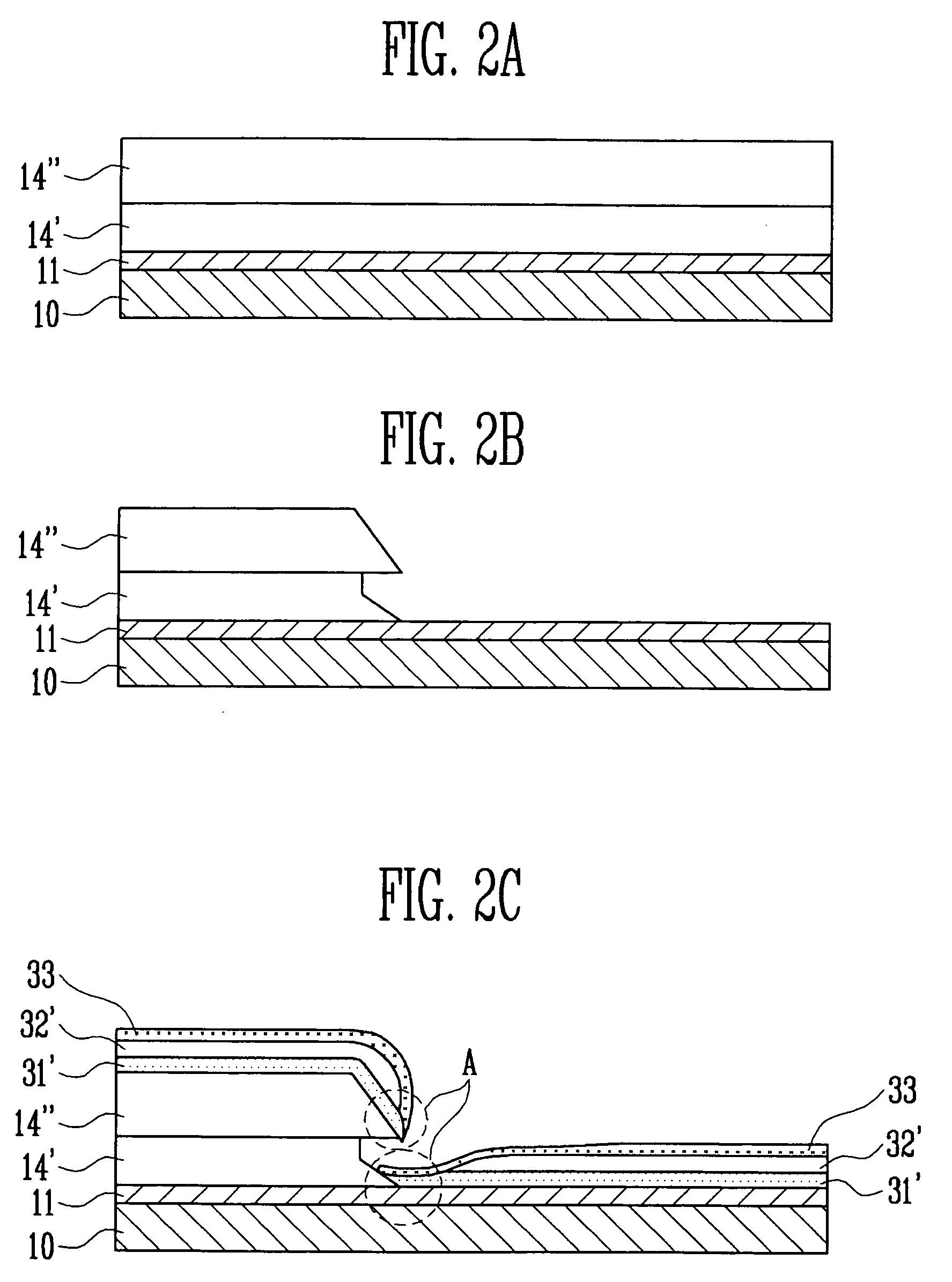
[0067]FIG. 3 is a cross-sectional view of an organic light emitting display according to the present invention.
[0068]The structure of the light emitting region is almost the same as the structure of the light emitting region described with reference to FIG. 1 except that the passivation layer 14 is formed in a single layer structure, not a double layer structure in the present embodiment, and therefore a detailed description thereof has been omitted. FIG. 3 is a cross section of only a portion of the non-light emitting region.
[0069]In the non-light emitting layer, the buffer layer 11 is formed on the first substrate 10, and at least two auxiliary electrode layers 40, 41 and 42 with different etch rates are formed on the buffer layer 11.
[0070]In the embodiment of the present invention, the structure that the auxiliary electrode layers 40, 41 and 42 formed of Mo / Al / Mo are sequentially stacked is described as an example.
[0071]In other words, the first auxiliary electrode layer 40 of Mo...
PUM
 Abstract
Description
Claims
Application Information