
NAND string based NAND/NOR flash memory cell, array, and memory device having parallel bit lines and source lines, having a programmable select gating transistor, and circuits and methods for operating same

a flash memory and array technology, applied in static storage, digital storage, instruments, etc., can solve the problem of increasing the number of external pins required by the program, and achieve the effect of removing the effect of program interference voltag

Inactive Publication Date: 2009-12-17
APLUS FLASH TECH
View PDF46 Cites 60 Cited by
  • Summary
  • Abstract
  • Description
  • Claims
  • Application Information

AI Technical Summary

Benefits of technology

[0020]Even further, another object of this invention is to provide a circuit and method for refreshing a nonvolatile memory cells within an array of nonvolatile memory cells to eliminate the effects of program disturb voltages.
[0029]During a program and erase operation, the fourth logic circuit is activated such that the output has logic state set so that blocks of the array of nonvolatile memory cells have their bit lines set to first or second high voltage power supply levels. In the erase operation, the global select signal associated with each column of the select gating charge retaining transistor is floating. This allows the coupling of a high erase voltage to be coupled to the gate of the first select gating charge retaining transistor from a well of a first conductivity type into which the selected block is formed to avoid an oxide breakdown during a Fowler-Nordheim erase operation.

Problems solved by technology

One disadvantage of NOR flash nonvolatile memory is as the density is doubled, the number of its required external pin count increases by one due to the adding of one more external address pin.

Method used


Image

  • NAND string based NAND/NOR flash memory cell, array, and memory device having parallel bit lines and source lines, having a programmable select gating transistor, and circuits and methods for operating same
  • NAND string based NAND/NOR flash memory cell, array, and memory device having parallel bit lines and source lines, having a programmable select gating transistor, and circuits and methods for operating same
  • NAND string based NAND/NOR flash memory cell, array, and memory device having parallel bit lines and source lines, having a programmable select gating transistor, and circuits and methods for operating same

Examples


Embodiment Construction

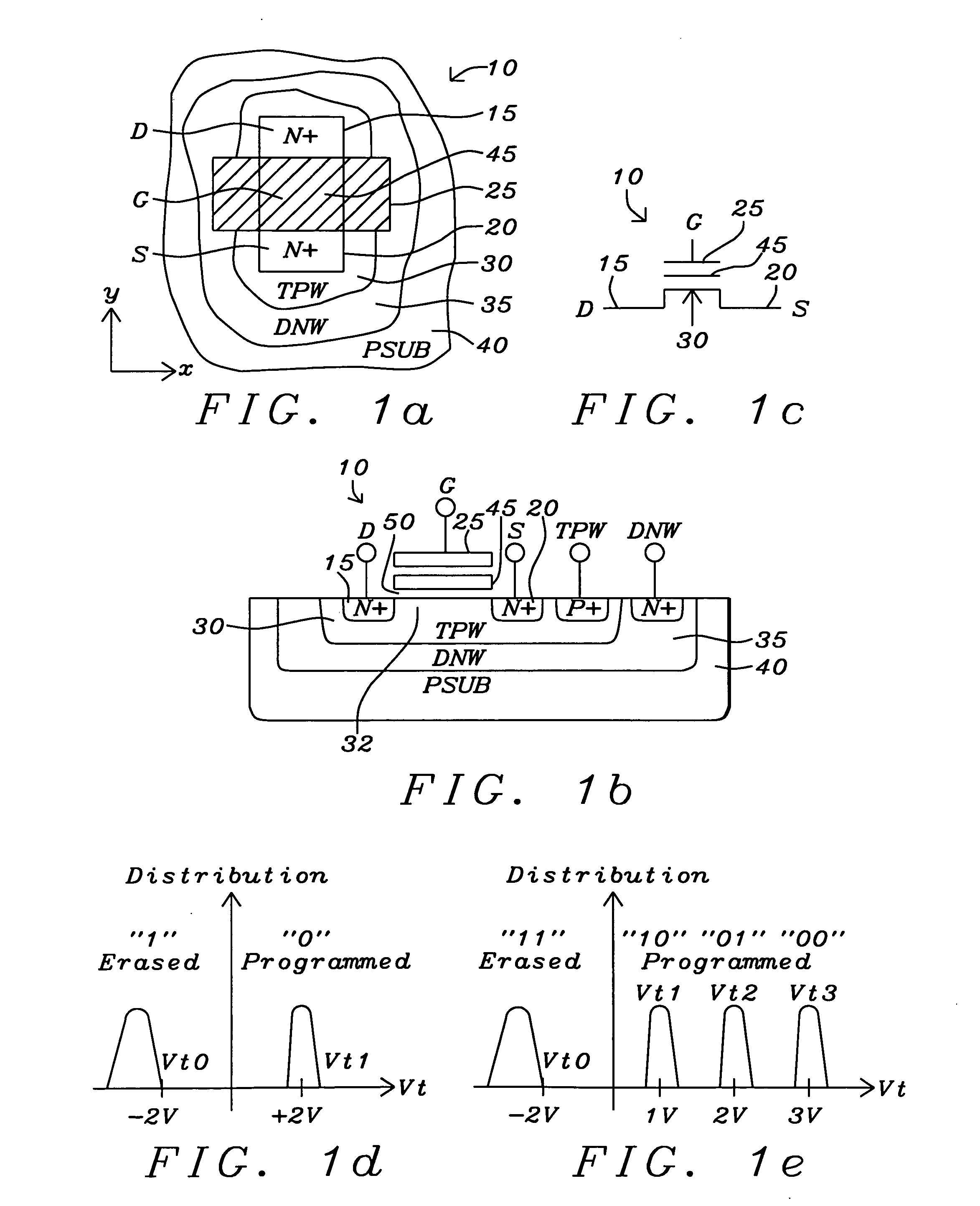
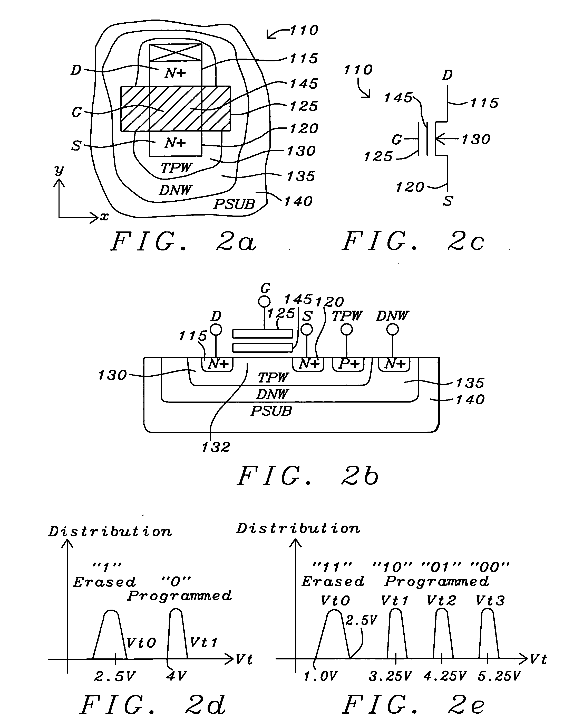
[0074]FIG. 1a is a top plan view of a NMOS NAND flash floating-gate transistor 10. FIG. 1b is a cross sectional view NMOS NAND flash floating-gate transistors 10. FIG. 1c is the schematic symbol NMOS NAND flash floating-gate transistors 10. In a common structure of a NAND cell string of the NMOS NAND flash floating-gate transistors 10, the NMOS NAND flash floating-gate transistors 10 do not require a contact at either the drain diffusion region 15 or source diffusion region 20 node. In conventional NAND cell strings have a top select transistor connected to the topmost transistor and a bottom select transistor connected to the bottommost transistor. The drain of the top select transistor and the source of the bottommost transistor have contacts for connected to bit lines and source lines. This structure for a conventional NAND string enables the size of the NMOS NAND flash floating-gate transistors 10 to be the smallest of the nonvolatile memory structures.

[0075]The floating-gate ty...


PUM


Abstract

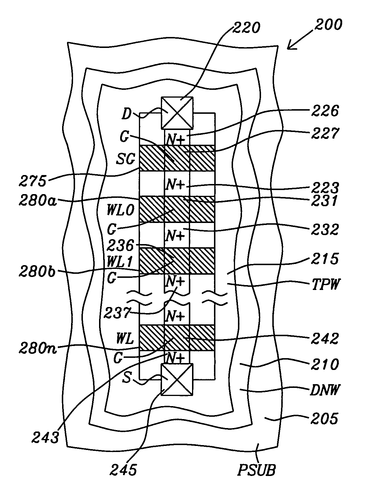
A nonvolatile memory device includes a nonvolatile memory array including a plurality of charge retaining transistors arranged in rows and columns. The device has a plurality source lines formed in parallel with the bit lines associated with each column. Row decode / driver circuits are connected to blocks of the charge retaining transistors for controlling the application of the necessary read, program, and erase signals. Erase count registers, each of the erase count registers associated with one block of the array of the charge retaining transistors for storing an erase count for the associated block for determining whether a refresh operation is to be executed. Groupings on each column of the array of charge retaining transistors are connected as NAND series strings where each NAND string has a select gating charge retaining transistor connected to the top charge retaining transistor for connecting the NAND series string to the bit lines.

Description

[0001]This application claims priority under 35 U.S.C. §119 to U.S. Provisional Patent Application U.S. Provisional Patent Application Ser. No. 61 / 130,381, filed on May 30, 2008, which is herein incorporated by reference in its entirety.[0002]This application claims priority under 35 U.S.C. §119 to U.S. Provisional Patent Application U.S. Provisional Patent Application Ser. No. 61 / 131,554, filed on Jun. 9, 2008, which is herein incorporated by reference in its entirety.[0003]This application claims priority under 35 U.S.C. §119 to U.S. Provisional Patent Application U.S. Patent Application Ser. No. 61 / 132,122, filed on Jun. 16, 2008, assigned to the same assignee as the present invention, and incorporated herein by reference in its entirety.[0004]This application claims priority under 35 U.S.C. §119 to U.S. Provisional Patent Application U.S. Patent Application Ser. No. 61 / 132,628, filed on Jun. 20, 2008, assigned to the same assignee as the present invention, and incorporated herei...

Claims


Application Information

Patent Timeline
IPC IPC(8): G11C16/04G11C16/06G11C16/16G11C8/00
CPCG11C8/12G11C8/14G11C11/5635G11C16/0483G11C2211/5644G11C16/3418G11C16/3427G11C16/3431G11C16/3436G11C16/10
Inventor LEE, PETER WUNGHSU, FU-CHANG
Owner APLUS FLASH TECH
Learn More