

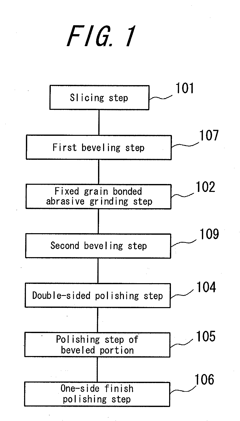
Method for producing semiconductor wafer
a technology of semiconductor wafers and machining allowances, which is applied in the direction of manufacturing tools, cutting machines, edge grinding machines, etc., can solve the problems of increased machining allowance of silicon materials, and increased machining allowance of semiconductor materials, so as to reduce the kerf loss of semiconductor materials, reduce the machining allowance of semiconductor wafers, and obtain semiconductor wafers cheaply
Inactive Publication Date: 2009-12-17
SUMCO CORP
View PDF20 Cites 18 Cited by
- Summary
- Abstract
- Description
- Claims
- Application Information
AI Technical Summary
Benefits of technology
[0012]It is, therefore, an object of the invention to advantageously solve the above-mentioned problems and to provide a method of producing a semiconductor wafer wherein both surfaces of a semiconductor wafer cut out from a crystalline ingot can be mirror-finished by employing a fixed grain bonded abrasive grinding step instead of the conventional lapping step and the one-side grinding step, and also the semiconductor wafer can be obtained cheaply by reducing the machining allowance of the semiconductor wafer to reduce the kerf loss of the semiconductor material. Particularly, the invention develops a remarkable effect when the semiconductor wafer is a silicon wafer having a diameter of not less than 450 mm.
[0013]In order to solve the above problems, the inventors have made various studies about a method for producing a semiconductor wafer wherein the number of production steps when a semiconductor wafer cut out from a crystalline ingot is rendered into a double-sided mirror-finished semiconductor wafer is decreased but also the silicon kerf loss in the semiconductor wafer is reduced as compared with those of the conventional method.
[0014]As a result, it has been found that the machining allowance of the semiconductor wafer can be reduced by conducting a fixed grain bonded abrasive grinding step of simultaneously conducting a treatment from rough grinding to finish grinding on both surfaces of the semiconductor wafer at once instead of the conventional lapping step and the one-side grinding step.
[0019]According to the production method of the semiconductor wafer according to the invention, a first beveling step and a fixed grain bonded abrasive grinding step are conducted between the slicing step and the double-sided polishing step, whereby the machining allowance of the semiconductor wafer can be reduced to reduce the kerf loss of the semiconductor material to thereby obtain the semiconductor wafer cheaply.
[0020]Also, the flatness of the semiconductor wafer can be improved by reducing the machining allowance of the semiconductor wafer. Furthermore, a semiconductor wafer having an epitaxial layer can be obtained by conducting an epitaxial layer growing step after the double-sided polishing step. The production method of the semiconductor wafer according to the invention is especially suitable for the production of semiconductor wafers having a diameter of not less than 450 mm.
Problems solved by technology
In the aforementioned conventional method, a double-sided mirror finished semiconductor wafer is produced through the two beveling steps, the lapping step and the one-side grinding step, so that there are problems that a kerf loss of a semiconductor material (loss of semiconductor material due to the increase of lapped scrap and one-side ground scrap) is brought about due to a large number of steps.
In the production method of the semiconductor wafer disclosed in this patent document, the problem of growing the size of the lapping apparatus in the production of the large-diameter semiconductor wafer is solved and the first beveling step before the double-sided grinding step can be omitted, but the double-sided grinding step and the one-side grinding step are conducted, and hence the machining allowance of the silicon material is still large, which remains as a problem about the kerf loss.
Method used
View moreImage
Smart ImageViewing Examples

Examples
invention example 1
[0070]A silicon wafer having a diameter of 300 mm is prepared according to a flow chart shown in FIG. 1 according to the invention.
invention example 2
[0071]A silicon wafer having a diameter of 450 mm is prepared in the same production method as in Invention Example 1.
example 1
CONVENTIONAL EXAMPLE 1
[0072]A silicon wafer having a diameter of 300 mm is prepared by a production method shown in FIG. 4 inclusive of a lapping step.
Login to View More PUM
| Property | Measurement | Unit |
|---|---|---|
| diameter | aaaaa | aaaaa |
| diameter | aaaaa | aaaaa |
| size | aaaaa | aaaaa |
Abstract
A semiconductor wafer is produced by a method comprising a slicing step, a fixed grain bonded abrasive grinding step and a beveling step, in which the kerf loss is reduced and the flatness is improved.
Description
BACKGROUND OF THE INVENTION[0001]1. Field of the Invention[0002]This invention relates to a method for producing a semiconductor wafer, and more particularly to a method for producing a semiconductor wafer by cutting out a thin disc-shaped semiconductor wafer from a crystalline ingot and then subjecting both surfaces thereof to a mirror finishing.[0003]2. Description of the Related Art[0004]The conventional method for producing a semiconductor wafer typically comprises a series of a slicing step→a first beveling step→a lapping step→a second beveling step→a one-side grinding step→a double-sided polishing step→a one-side finish polishing step in this order.[0005]In the slicing step, a thin disc-shaped semiconductor wafer is cut out from a crystalline ingot. In the first beveling step, an outer peripheral portion of the cut semiconductor wafer is beveled to suppress the occurrence of cracking or chipping in the semiconductor wafer at the subsequent lapping step. In the lapping step, th...
Claims
Login to View More Application Information
Patent Timeline
 Patent Type & AuthorityApplications(United States)
IPC IPC(8): B24B7/26B28D1/02B24B9/06B24B1/00B24B37/08H01L21/304
CPCB24B7/17B28D5/0005B24B7/228
InventorHASHII, TOMOHIROKAKIZONO, YUICHI
OwnerSUMCO CORP