Dislocation-based light emitter

a technology of dislocation and light emitting, which is applied in the direction of semiconductor lasers, semiconductor devices, electrical equipment, etc., can solve the problems of not being given any chance of use, not being integrated into silicon-based semiconductor technology, and complicated and expensive hybrid processes

Inactive Publication Date: 2009-12-31
IHP GMBH INNOVATIONS FOR HIGH PERFORMANCE MICROELECTRONICS LEIBNIZ INST FUR INNOVATIVE
View PDF3 Cites 3 Cited by
  • Summary
  • Abstract
  • Description
  • Claims
  • Application Information

AI Technical Summary

Benefits of technology

[0016]Surprisingly it has been found that setting suitable pairs of twist angles and tilt angles provides for the formation of dislocation networks at the first interface, which cause a spectrally limited and intensive luminescence which, depending on the respective pair of angles, is caused quite predominantly by the D1-emission or by the D3-emission. In that respect the D1-luminescence covers the spectral range around 1.55 micrometers and the D3-luminescence covers the spectral range around 1.3 micrometers. By virtue of the suppression of competing radiant energy relaxation processes, which is achieved at the same time, the quantum efficiency of the light emission in the respectively optimized luminescence range, that is to say either in the range of the D1-luminescence or in the range of the D3-luminescence, is increased.
[0021]The light-emitting semiconductor component of this embodiment makes it possible to markedly emphasize the D1-emission with respect to the D2 through D4-emissions and with respect to the band-band emission line at 1.1 eV. The spectral width of the electroluminescence of the semiconductor component is markedly reduced in that way. In addition, the quantum efficiency of the light emission in the range of the D1-luminescence is increased by virtue of the suppression of competing radiant energy relaxation processes.
[0029]In regard to the intensity of the D1-light emission, it has proven to be advantageous if slight decoration of the dislocation network with oxygen is involved.
[0036]In a further embodiment the efficiency of D1-emission or D3-emission is further increased by the substrate including two or more interfaces at which a corresponding dislocation network is formed. By virtue of the complexity of manufacture, a semiconductor component with two influences is preferred, wherein the second silicon layer at its side remote from the first silicon layer forms with a third silicon layer a second interface at which the second and third silicon layers are rotated relative to each other through a second twist angle and are tilted through a second tilt angle, in such a way that a dislocation network is present in the region of the second interface, wherein the second twist angle and the second tilt angle are so selected that an electroluminescence spectrum of the semiconductor component from the region of the second dislocation network has an absolute maximum of the emitted light intensity at either 1.3 micrometers light wavelength or 1.55 micrometers light wavelength.
[0039]A preferred embodiment of the light-emitting semiconductor component has an n-doped portion and a p-doped portion adjoining same. They are preferably arranged relative to the first interface or the first and second interfaces in such a way that the dislocation network, or the dislocation networks when there are a plurality of interfaces, lies or lie outside a barrier layer which is formed at forward polarity of the semiconductor component. In that way a high concentration of excess charge carriers can be achieved in the light-emitting region at the dislocation networks near the interfaces. In an alternative embodiment there are provided an n-doped portion and a p-doped portion adjoining same, which are so arranged relative to the first interface or the first and second interfaces that the dislocation network or networks lie within a barrier layer formed upon forward polarity of the semiconductor component.

Problems solved by technology

They can only be integrated into the silicon-based semiconductor technology, in the form of complicated and expensive hybrid processes.
Such processes are not given any chances of use.
The low level of defects required for the necessary light yield however can only be implemented with difficulty when using such alloys.
A disadvantage of the light-emitting diodes described by Kveder et al. is that their luminescence extends over a relatively wide spectral range and also has a pronounced shoulder at higher energy levels around 0.85 eV.
It is however of no interest for optoelectronic uses.
The plastically deformed substrates used by Kveder et al. for the production of the light-emitting diodes also suffer from the disadvantage that the irregular dislocation arrangements contained therein, in accordance with the present state of the art, cannot be adequately reproducibly produced.

Method used


Image

  • Dislocation-based light emitter
  • Dislocation-based light emitter
  • Dislocation-based light emitter

Examples


Embodiment Construction

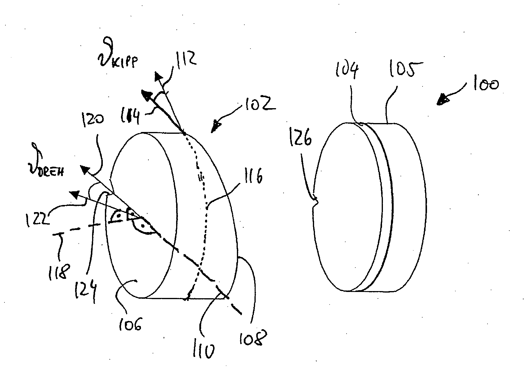
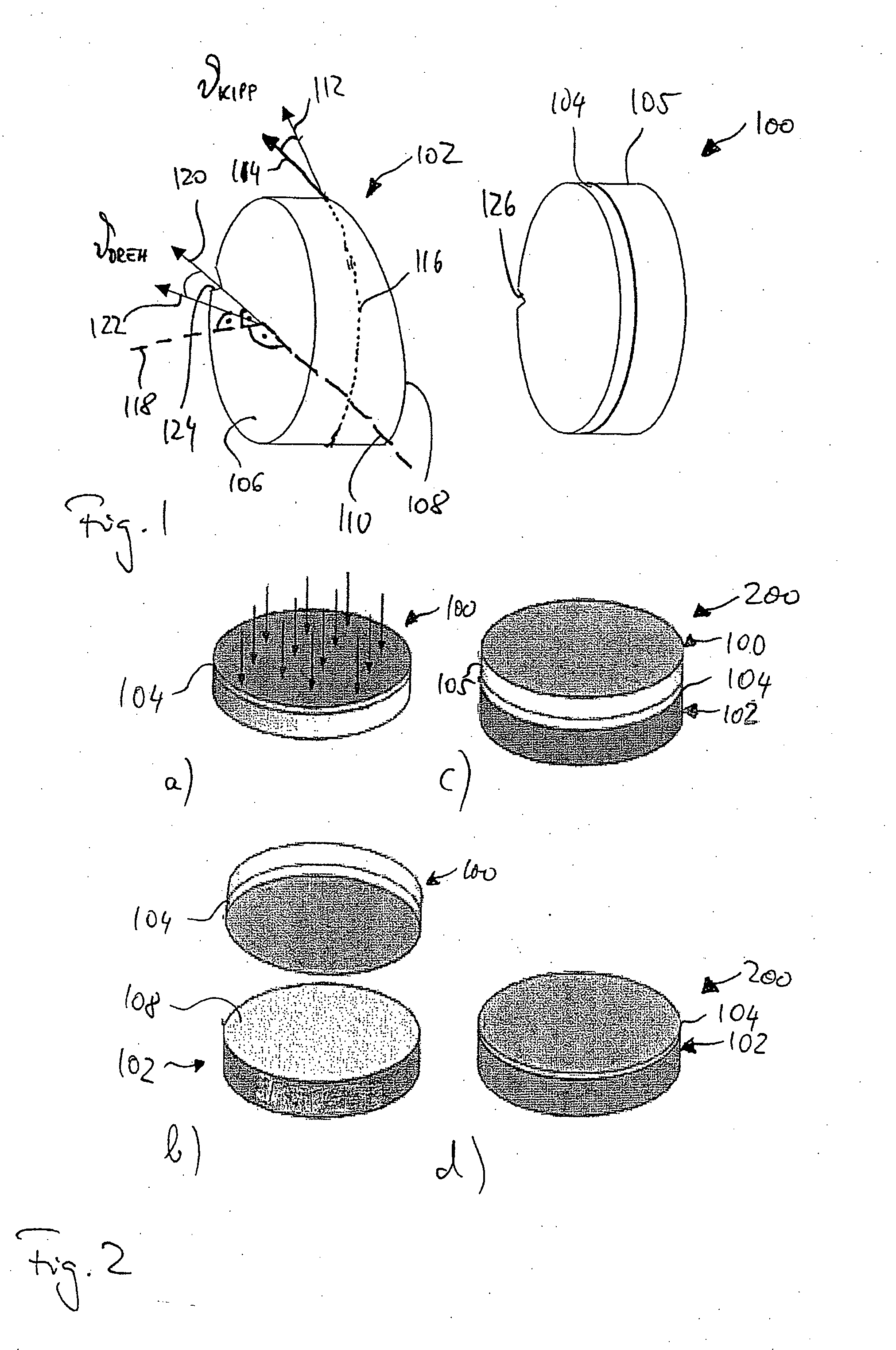
[0053]FIG. 1 is a diagrammatic three-dimensional view showing two wafers 100 and 102 which are used for the production of the substrate of a light emitter according to the invention.

[0054]The wafer 100 is a (100)-silicon wafer into which hydrogen ions or helium ions are introduced by a hydrogen implantation step with a dose of between 1×10¹⁶−1×1017 cm−2. The implanted layer 104 extends over a depth of about 200 nm from the substrate surface.

[0055]The wafer 102 is also a (100)-silicon wafer. Unlike the wafer 100 however its two surfaces 106 and 108 are not parallel to each other but tilted relative to each other through a small angle θKIPP. That angle is referred to as the “tilt”. The axis about which the surface 108 is tilted relative to the surface 106 is parallel to the -direction and is indicated by a broken line 110. The angle θKIPP between an arrow 112 extending parallel to the surface 106 and an arrow 114 extending parallel to the surface 108 is shown for the sake of clarity. ...


PUM


Abstract

A light-emitting semiconductor component comprising a substrate which has a first interface between a first and a second silicon layer, whose lattice structures which are considered as ideal are rotated relative to each other through a twist angle about a first axis perpendicular to the substrate surface and are tilted through a tilt angle about a second axis parallel to the substrate surface, in such a way that a dislocation network is present in the region of the interface, wherein the twist angle and the tilt angle are so selected that an electroluminescence spectrum of the semiconductor component has an absolute maximum of the emitted light intensity at either 1.3 micrometers light wavelength or 1.55 micrometers light wavelength.

Description

CROSS REFERENCE TO RELATED APPLICATIONS[0001]This application is for entry into the U.S. national phase under §371 for International Application No. PCT / EP2006 / 062030 having an international filing date of May 3, 2006, and from which priority is claimed under all applicable sections of Title 35 of the United States Code including, but not limited to, Sections 120, 363 and 365(c), and which in turn claims priority under 35 USC §119 to German Patent Application No. 10 2005 008 025.4 filed on Feb. 16, 2006, and German Patent Application No. 10 2005 021 296.4 filed on May 3, 2005.BACKGROUND OF THE INVENTION[0002]1. Technical Field[0003]The present invention concerns the field of semiconductor components. More particularly, the present invention concerns a silicon-based light-emitting semiconductor component and a process for the production of such a light-emitting semiconductor component.[0004]2. Discussion of Related Art[0005]The development in semiconductor technology is going in the ...

Claims


Application Information

Patent Timeline
Patent Type & Authority Applications(United States)
IPC IPC(8): H01L33/00H01L33/16H01L33/34
CPCH01L33/16H01S5/3227H01S5/3224H01L33/34
Inventor KITTLER, MARTINREICHE, MANFREDARGUIROV, TZANIMIRSEIFERT, WINFRIED
Owner IHP GMBH INNOVATIONS FOR HIGH PERFORMANCE MICROELECTRONICS LEIBNIZ INST FUR INNOVATIVE
Why Eureka
Try Eureka