Semiconductor device, integrated circuit, and semiconductor manufacturing method

a semiconductor and integrated circuit technology, applied in the direction of semiconductor devices, electrical appliances, transistors, etc., can solve the problems of reducing the effect of lowering the power consumption of lsi in lowering vdd, increasing the sub-threshold current flowing across the source and drain, and affecting the manufacturing of thin channel misfets having a thin channel film thickness, etc., to achieve the effect of suppressing the effect of variation of the threshold voltag

Inactive Publication Date: 2009-12-31
RENESAS ELECTRONICS CORP
View PDF1 Cites 132 Cited by
  • Summary
  • Abstract
  • Description
  • Claims
  • Application Information

AI Technical Summary

Benefits of technology

[0033]According to the present invention, with an integrated circuit having a plurality of MISFETs formed from semiconductor layers on an insulation film, it is possible to suppress the effects of variation of a threshold voltage caused by the influence of statistical variation from designed values for channel film thickness and variation of volume concentration in a depth direction from a channel film surface of the impurities.

Problems solved by technology

Lowering of the threshold voltage causes an increase in sub-threshold leakage current flowing across the source and drain when the FET is off.
As a result, the benefits of reduced power consumption of the LSI in lowering Vdd is degraded.
Not only the manufacturing of thin-film channel MISFETs having a thin channel film thickness become difficult, but also variation in element characteristics of the device become substantial with respect to deviation in channel film thickness.

Method used


Image

  • Semiconductor device, integrated circuit, and semiconductor manufacturing method
  • Semiconductor device, integrated circuit, and semiconductor manufacturing method
  • Semiconductor device, integrated circuit, and semiconductor manufacturing method

Examples


first embodiment

[0099]Next, a description is given of a semiconductor device and an integrated circuit of the present invention. FIG. 9 is a cross-sectional view showing a configuration for a thin-film channel MISFET of this embodiment.

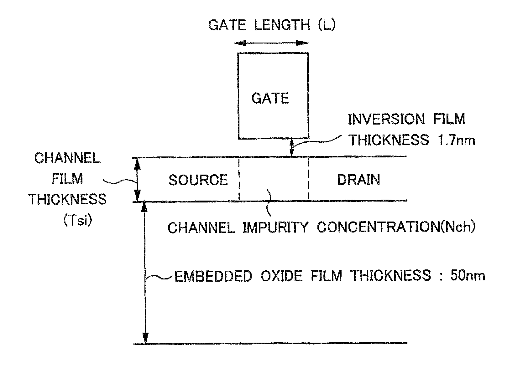
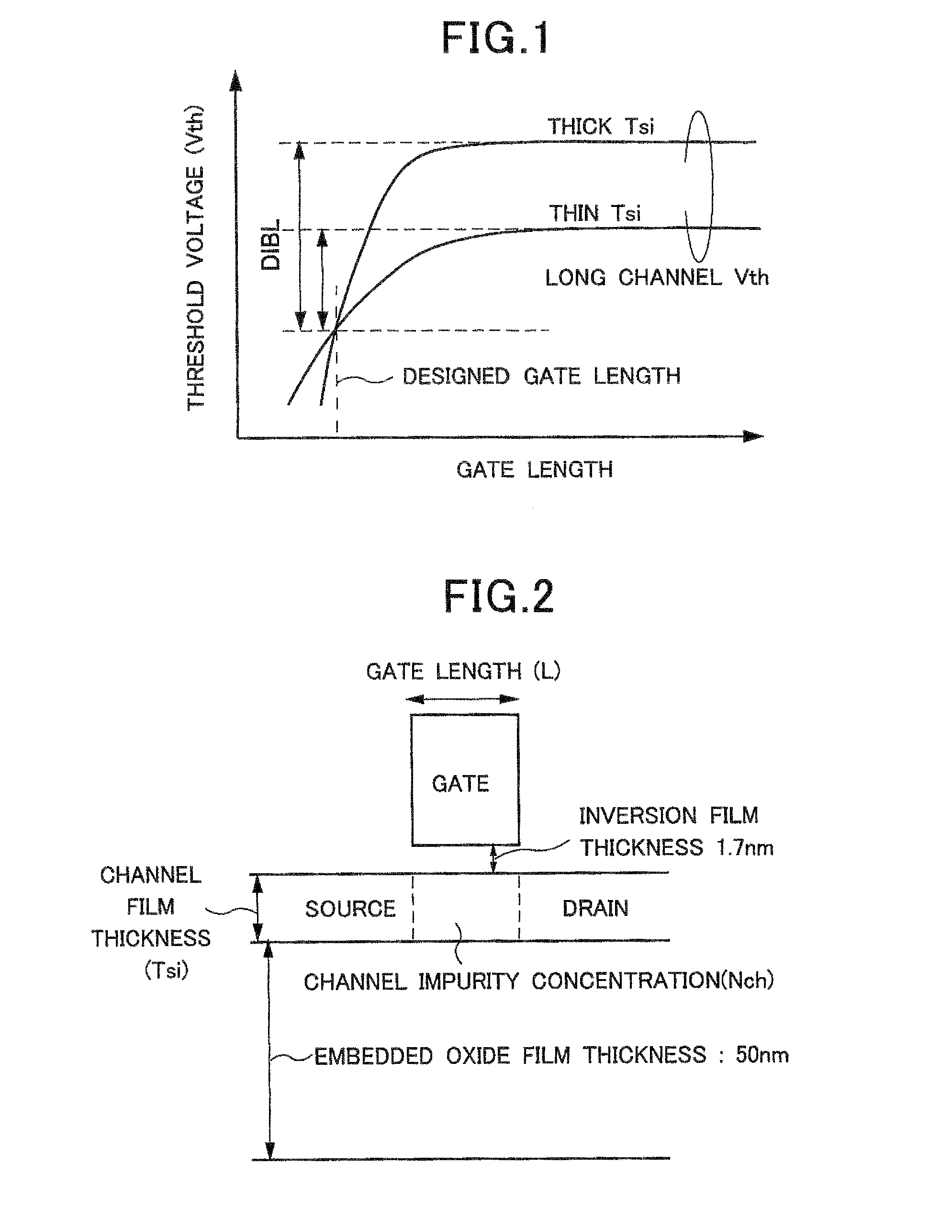
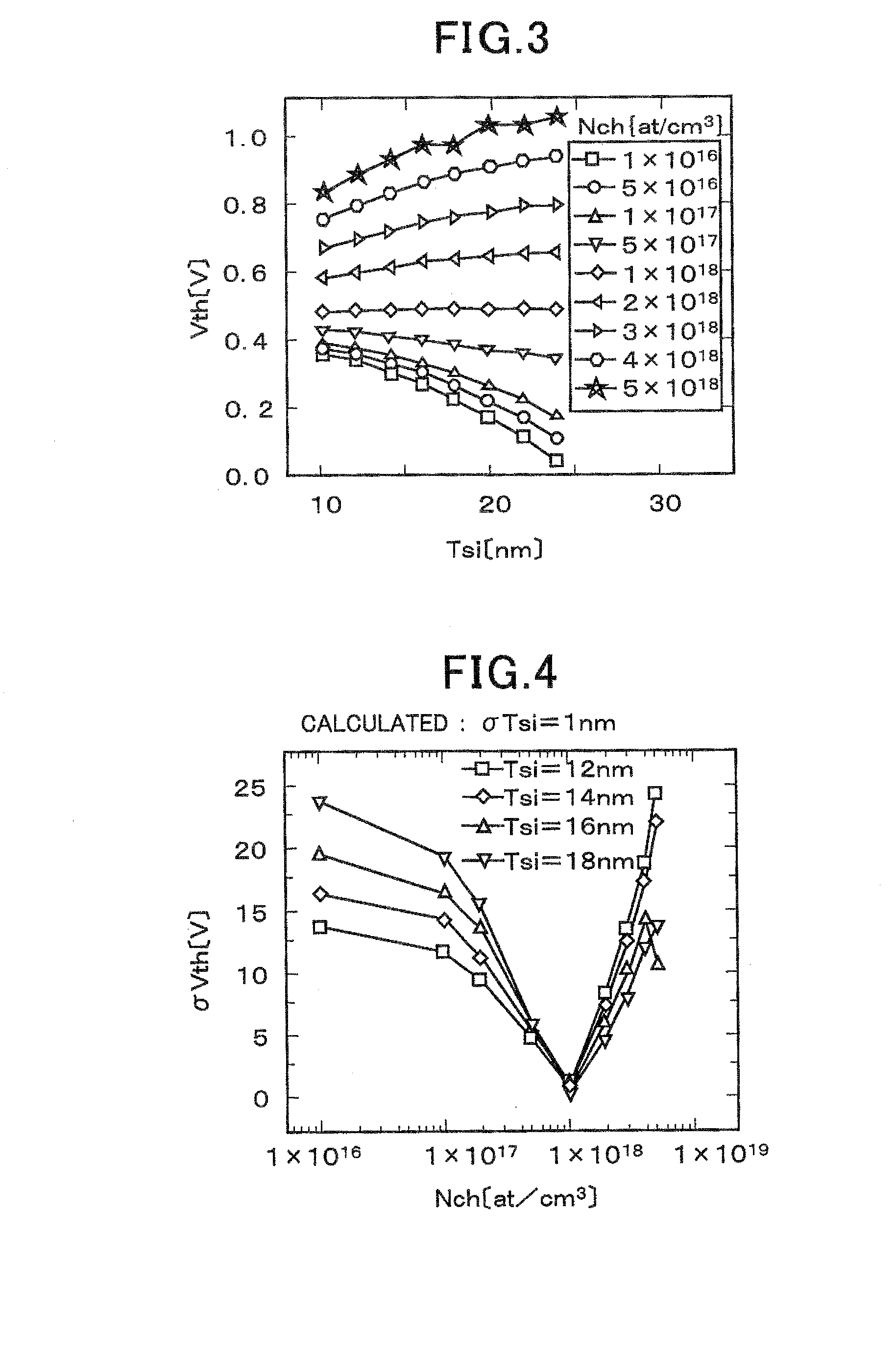
[0100]As shown in FIG. 9, an SOI structure is formed for a thin-film channel MISFET of this embodiment by sequentially forming an embedded oxide film 2 and a silicon thin-film 3 on a semiconductor substrate 1. An element separation region 4 is formed on the embedded oxide film 2 using trench separation. Source / drain diffusion layers 5 and 6 and a channel region 7 provided between the diffusion layers are formed on the silicon thin-film 3 within the element separation region 4. Impurities of a prescribed concentration are then uniformly introduced in a depth direction at the channel region 7. At the designed gate length, the volume concentration of this impurity is a concentration that minimizes variation in threshold voltage caused by variation in channel film thickn...

second embodiment

[0108]Next, a description is given of a method for manufacturing a semiconductor device of the present invention. FIGS. 10A to 10C are cross-sectional views showing an order of steps of a method for manufacturing this embodiment, and FIGS. 11D to 11F are cross-sectional views showing an order of steps for the method of manufacturing this embodiment continuing on from FIG. 10. The following is a description of an example of a method for manufacturing a P-type MOSFET. However, it is also possible to make an N-type MOSFET by appropriately selecting the ion species and injection energy etc.

[0109]First, as shown in FIG. 10A, an embedded oxide film 22 and a silicon thin-film 23 are sequentially formed one on top of the other on a silicon substrate 21. An element separation region 24 is then formed on the embedded oxide film 22 using trench separation.

[0110]Next, as shown in FIG. 10B, a sacrifice oxide film 25 is formed on the silicon thin-film 23 and the element separation region 24 withi...

third embodiment

[0131]Next, a description is given of a method for manufacturing a semiconductor device of the present invention. In this embodiment, a method of manufacturing a FinFET is disclosed where the concentration per unit area of impurity contained in the thin-film channel region becomes larger for MISFETs where the channel film thickness is thicker and the impurity concentration per unit volume is set to become greater in a depth direction from the channel film surface.

[0132]A description is now given of a method for manufacturing a semiconductor device of this embodiment with reference to FIGS. 20 and 21. FIGS. 20A to 20D are cross-sectional views showing the order of steps of the method for manufacturing the semiconductor device of the third embodiment. FIGS. 21E to 21G are cross-sectional views showing the order of steps of the manufacturing method continuing on from FIG. 20. First, as shown in FIG. 20A, an embedded oxide film 82, and a silicon film 83 introduced with impurities of a p...


PUM


Abstract

A semiconductor circuit has a plurality of MISFETs formed with channel films comprised of semiconductor layers on an insulation film. Channel film thicknesses of each MISFET are different. A correlation relationship is fulfilled where concentration per unit area of impurity contained in the channel films becomes larger for MISFETs of a thicker channel film thickness. As a result, it is possible to suppress deviation of threshold voltage caused by changes in channel film thickness. In this event, designed values for the channel film thicknesses of the plurality of MISFETs are preferably the same, and the difference in channel film thickness of each MISFET may depend on statistical variation from the designed values. The concentration of the impurity per unit area is proportional to the channel film thickness, or is a function that is convex downwards with respect to the channel film thickness.

Description

TECHNICAL FIELD [0001]The present invention relates to a semiconductor device, an integrated circuit, and a method for manufacturing a semiconductor device suitable for lowering variation in a threshold voltage of a MISFET (Metal Insulator Semiconductor Field Effect Transistor) having a thin-film channel.BACKGROUND ART[0002]In order to improve various characteristics of a large-scale integration circuit such as increasing the degree of integration and increasing the speed of operation, MOS Field Effect Transistors (MOSFET: Metal Oxide Semiconductor Field Effect Transistor), that are a basic configuration element of a large-scale integration (LSI: Large Scale Integration) circuit, are being miniaturized. This miniaturization is carried out in accordance with scaling that simultaneously reduces three-dimensional dimensions of the elements.[0003]An important requirement of MOSFET scaling is that, together with the miniaturization of the actual three-dimensional dimensions, a potential ...

Claims


Application Information

Patent Timeline
Patent Type & Authority Applications(United States)
IPC IPC(8): H01L27/088H01L21/8234
CPCH01L21/823412H01L21/845H01L27/1211H01L29/105H01L29/78696H01L29/785H01L29/78648H01L29/78654H01L29/66772H01L21/84H01L27/1203
Inventor MIYAMURA, MAKOTOTAKEUCHI, KIYOSHI
Owner RENESAS ELECTRONICS CORP
Why Eureka
Try Eureka