Graphene pattern and process of preparing the same

a graphene pattern and graphene technology, applied in the field of graphene patterns, can solve the problems of inability to develop a simple process for separating single-walled carbon nanotubes, inability to economically and reproducibly prepare a large-area graphene sheet, and high cost of products made from carbon nanotubes which are similar to graphene sheets

Active Publication Date: 2009-12-31
SAMSUNG ELECTRONICS CO LTD
View PDF11 Cites 74 Cited by
  • Summary
  • Abstract
  • Description
  • Claims
  • Application Information

AI Technical Summary

Problems solved by technology

Also, it is advantageous to use graphene sheets since products made from graphite are inexpensive while products made from carbon nanotubes which are similar to graphene sheets are expensive due to low yields obtained during synthesis and purification processes even though the carbon nanotubes are inexpensive themselves.
However, separating single wall carbon nanotubes is not a simple process.
However, although the graphene sheet has these advantageous characteristics, a method of economically and reproducibly preparing a large-area graphene sheet has not been developed yet.
In this case, the separated graphene sheet does not include a uniform number of layers, and does not have a uniform shape of tipped portions.
Furthermore, a large-area graphene sheet cannot be prepared.
However, the SiC single crystal which is used as a starting material used in the SiC thermal decomposition is very expensive, and a large-area graphene sheet cannot be easily prepared.
Therefore, it is not easy to prepare a graphene sheet, and the graphene sheet cannot be easily patterned on a substrate.

Method used


Image

  • Graphene pattern and process of preparing the same
  • Graphene pattern and process of preparing the same
  • Graphene pattern and process of preparing the same

Examples


example 1

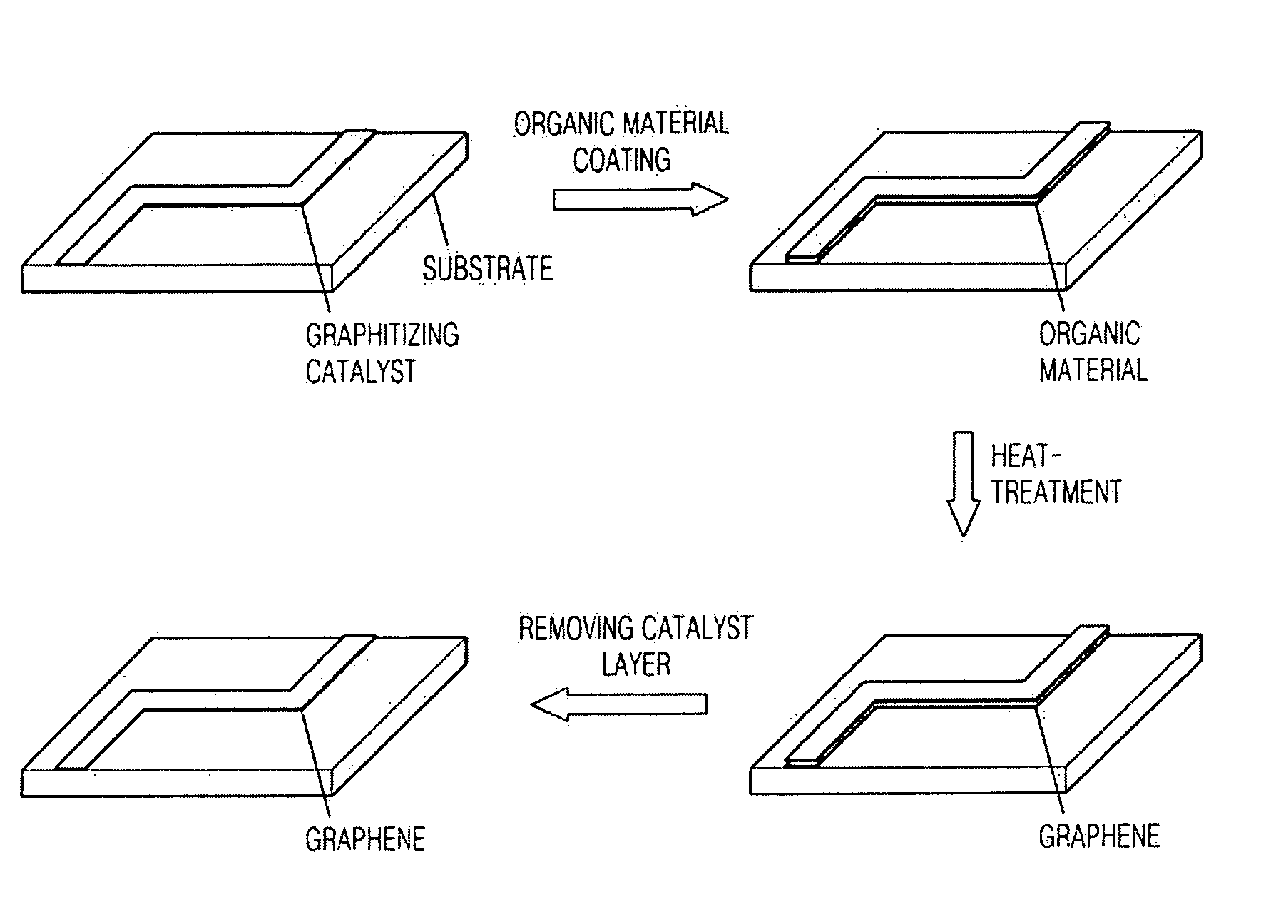
[0089]A photoresist (PR) patterning was formed on a 3 cm×3 cm silicon substrate on which 100 nm of SiO2 is coated, and Ni was deposited using sputtering to form a Ni high-precision pattern having a line width of 1 micron.

[0090]An oleic acid solution was separately prepared by dissolving oleic acid in chloroform to a concentration of 1 mg / ml. After water is added to a LB device, 50 μl of the oleic acid solution was dropped thereto. Then, a self assembled monolayer (SAM) was prepared using the LB device. The SAM formed of oleic acid was polymerized by radiating UV rays of a wavelength of 254 nm. The polymerized oleic acid SAM was transferred to the silicon substrate on which 100 nm of SiO2 is coated.

[0091]Then, the oleic acid-coated substrate was dried by heating at 60° C. for 12 hours in a vacuum atmosphere. The dried oleic acid-coated substrate was heat-treated in a furnace at 500° C. for 1 hour in a nitrogen atmosphere to obtain a substrate including a single-layered graphene sheet...

example 2

[0093]A substrate including a 4-layered graphene pattern was prepared in the same manner as in Example 1, except that the process of transferring the polymerized oleic acid SAM to the Ni pattern was repeated 4 times.

[0094]Then, the substrate on which the graphene pattern is formed was melted in 0.1 M HCl for 24 hours to remove the Ni thin film.

example 3

[0095]Ni was deposited on a 3 cm×3 cm silicon substrate on which 100 nm of SiO2 is coated using sputtering to form a Ni thin film.

[0096]An oleic acid solution was separately prepared by dissolving oleic acid in chloroform to a concentration of 1 mg / ml. After water is added to a LB device, 50 μl of the oleic acid solution was dropped thereto. Then, a self assembled monolayer (SAM) was prepared using the LB device. The SAM formed of oleic acid was polymerized by radiating UV rays of a wavelength of 254 nm. The polymerized oleic acid SAM was transferred to the silicon substrate on which 100 nm of SiO2 is coated. The process of transferring the polymerized oleic acid SAM to the substrate was repeated 4 times.

[0097]The substrate was partially heat-treated using e-beam to form a 4-layered graphene having a line width of 50 nm, and melted in 0.1 M HCl for 24 hours to remove the oleic acid SAM formed on the region on which graphene is not formed and the Ni thin film.


PUM

PropertyMeasurementUnit
temperatureaaaaaaaaaa
thicknessaaaaaaaaaa
boiling pointaaaaaaaaaa

Abstract

Provided are a graphene pattern and a process of preparing the same. Graphene is patterned in a predetermined shape on a substrate to form the graphene pattern. The graphene pattern can be formed by forming a graphitizing catalyst pattern on a substrate, contacting a carbonaceous material with the graphitizing catalyst and heat-treating the resultant.

Description

CROSS-REFERENCE TO RELATED PATENT APPLICATION[0001]This application claims the benefit of Korean Patent Application No. 10-2007-0094895, filed on Sep. 18, 2007 and 10-2008-0023458, filed on Mar. 13, 2008, in the Korean Intellectual Property Office, the disclosure of which is incorporated herein in its entirety by reference.BACKGROUND OF THE INVENTION[0002]1. Field of the Invention[0003]The present invention relates to a graphene pattern and a process of preparing the same, and more particularly, to a graphene pattern formed in a predetermined shape on a substrate and a process of easily preparing the graphene pattern.[0004]2. Description of the Related Art[0005]Generally, graphite is a stack of two-dimensional graphene sheets formed from a planar array of carbon atoms bonded into hexagonal structures. Recently, as a result of testing properties of single-layered or several-layered graphene sheets, their beneficial properties have been revealed.[0006]The most noticeable beneficial pr...

Claims


Application Information

Patent Timeline
Patent Type & Authority Applications(United States)
IPC IPC(8): B32B3/10B05D1/18
CPCB81B2207/056Y10T428/24851B82Y30/00B82Y40/00C01B31/0461H01L29/1606H01L29/43H05K3/105H05K2201/0323C30B19/08C30B19/12C30B25/10C30B25/18C30B29/02C30B29/64Y10S977/734Y10S977/842Y10S977/843Y10T428/24802Y10T428/24917B81C1/00031C01B32/188C01B32/00
Inventor CHOI, JAE-YOUNGSHIN, HYEON-JINYOON, SEON-MI
Owner SAMSUNG ELECTRONICS CO LTD
Why Eureka
Try Eureka