Light-emitting display device

a display device and light-emitting technology, applied in the field of light-emitting display devices, can solve the problems of change in the characteristics of the tft due to electrical stress, the voltage-luminance characteristic of the oled element changes, and the oled element's voltage-luminance characteristic is changed temporally, so as to achieve high mobility, low power consumption, and high definition.

Active Publication Date: 2010-01-07
CANON KK
View PDF14 Cites 67 Cited by
  • Summary
  • Abstract
  • Description
  • Claims
  • Application Information

AI Technical Summary

Benefits of technology

[0034]According to the present invention, an n-type TFT whose channel layer is a metal oxide semiconductor layer having a carrier density equal to or smaller than 1018 (cm−3), a field effect mobility equal to or larger than 1 (cm2 / Vs), and an on / off ratio equal to or larger than 106 is used as the n-type TFT. Therefore, as compared with the case of a structure using the a-Si or OS TFT, it is possible to produce a light-emitting display device using a TFT which has low power consumption and can be formed at room temperature. Because of high mobility, a necessary TFT size is small, so high definition can be realized.
[0035]According to the present invention, the n-type TFT whose channel layer is an amorphous metal oxide semiconductor layer is used. Therefore, because of the amorphous layer, it is possible to produce a TFT whose flatness is high and variations in characteristics are small.

Problems solved by technology

In the AM OLED display, there is a problem of a temporal change in voltage-luminance characteristic of the OLED element.
Also, there are problems in that variations in characteristics of the TFTs and changes in characteristics of the TFT due to electrical stress occur.
However, because of crystal grain boundary, variations in characteristics are more likely to increase and a manufacturing cost becomes larger.
On the other hand, an a-Si or OS TFT has lower mobility than the p-Si TFT, so the operating voltage is high and thus power consumption is large.
Unlike the p-Si TFT, it is difficult to use the a-Si, OS, or metal oxide semiconductor TFT for a complementary TFT in which an n-type TFT and a p-type TFT are formed on the same substrate.
For example, in the case of a-Si or metal oxide, a high-mobility p-type semiconductor is not obtained, so it is difficult to form the p-type TFT.
In the case of OS, because a high-mobility n-type semiconductor material is different from a high-mobility p-type semiconductor material, the number of steps is doubled, so low-cost manufacturing is difficult to achieve.
A large-size and high-definition OLED display is required, so it tends to increase a line load.
Thus, it is difficult to apply the drive circuit described in Japanese Patent Application Laid-open No. 2004-093777 to a high-definition and large-screen display device.
However, it is insufficient to use the drive circuit for the high-definition television.
However, in the circuit, the voltage between the gate terminal and the source terminal of the driving TFT is not fixed.

Method used


Image

  • Light-emitting display device
  • Light-emitting display device
  • Light-emitting display device

Examples


first embodiment

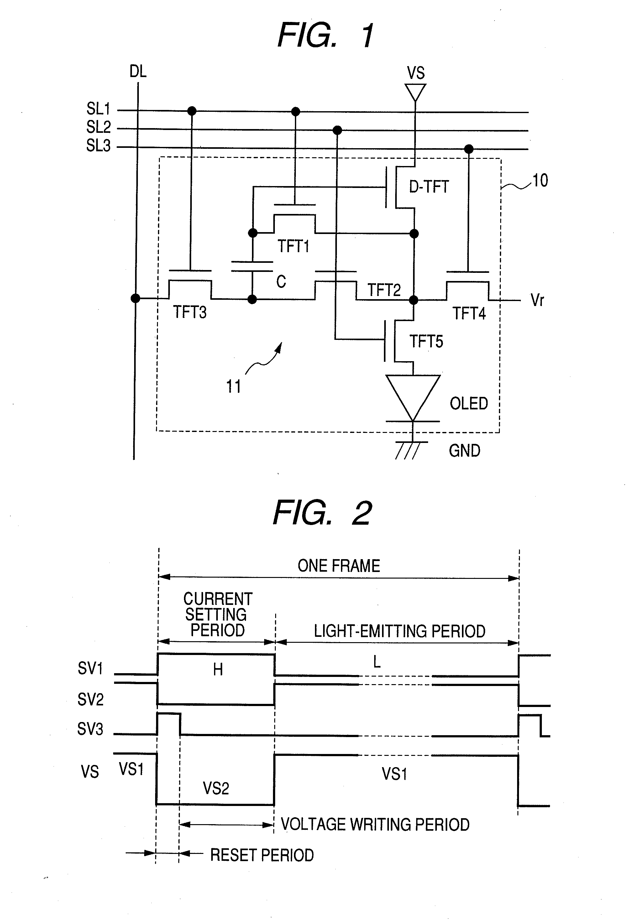
[0064]FIG. 1 illustrates a pixel structure of a light-emitting display device using an OLED element (hereinafter, referred to as OLED display) according to a first embodiment of the present invention.

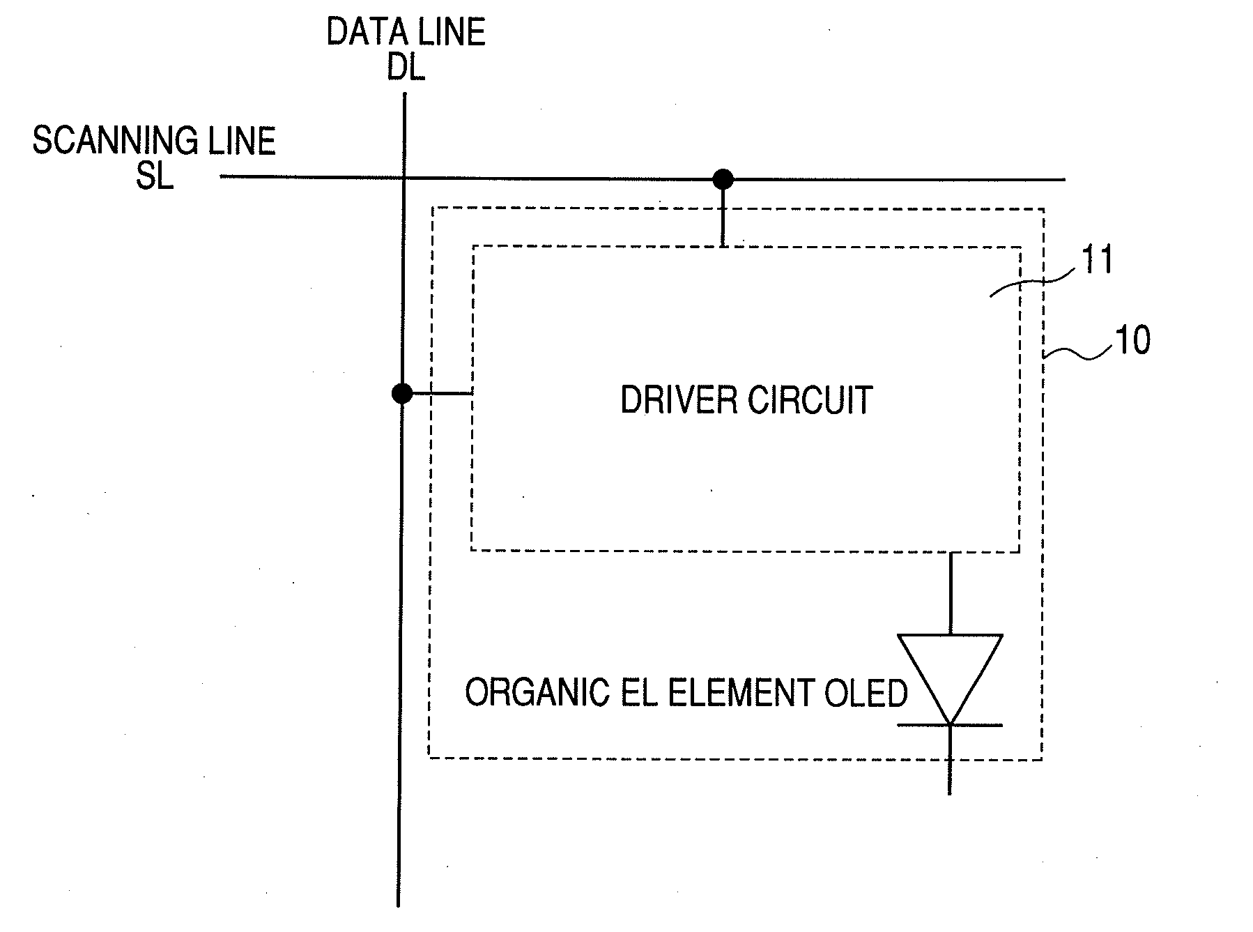
[0065]The OLED display according to this embodiment has each pixel 10 which includes an OLED element whose cathode terminal is connected (grounded) with a GND (ground) line (hereinafter, referred to as GND) and a drive circuit 11 connected with an anode terminal of the OLED.

[0066]The OLED has a structure in which a light-emitting layer made of an organic material is sandwiched between the anode terminal and the cathode terminal and emits light at a luminance corresponding to a current supplied from the drive circuit 11. The current supplied from the drive circuit 11 to the OLED is determined based on a control voltage from a data line.

[0067]The drive circuit 11 includes a driving transistor having a gate terminal, a source terminal, and a drain terminal, for driving the OLED, a capacito...

second embodiment

[0098]A pixel structure of a light-emitting display device using an OLED element according to a second embodiment of the present invention is similar to the pixel arrangement of the first embodiment. Note that, in this embodiment, the voltage VS2 of the power supply line VS is a constant value. When the threshold voltage of the D-TFT is expressed as Vt, “Vref−Vt>VS2” is satisfied. In other words, a highest voltage other than the voltage signals SV1, SV2, and SV3 of the first, second, and third scanning lines SL1, SL2, and SL3 is the reference voltage Vref of the reference voltage line Vr. The voltage VS2 of the power supply line VS is set to such a voltage that the D-TFT operates in the saturation region when the current is supplied to the OLED.

[0099]FIG. 3 is a timing chart illustrating an operation in this embodiment. The operation in this embodiment is similar to the operation in this first embodiment except that the voltage VS2 of the power supply line VS is the constant value a...
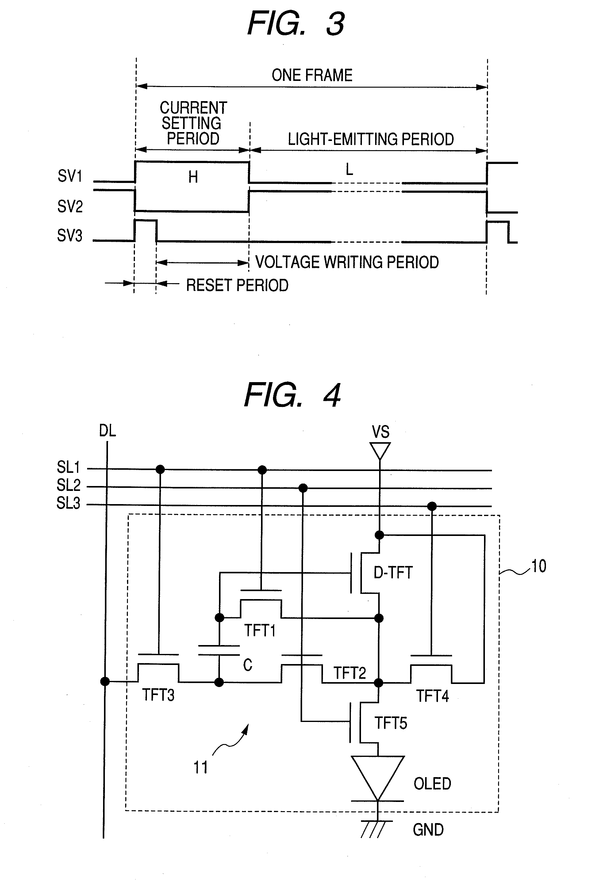
third embodiment

[0101]FIG. 4 illustrates a pixel structure of a light-emitting display device using an OLED element according to a third embodiment of the present invention. The description of the same constituent elements as the first embodiment is simplified or omitted.

[0102]The OLED display according to this embodiment has each pixel 10 which includes an OLED element whose cathode terminal is connected (grounded) with a GND (ground) line (hereinafter, referred to as GND) and a drive circuit 11 connected with an anode terminal of the OLED.

[0103]The drive circuit 11 includes a driving transistor having a gate terminal, a source terminal, and a drain terminal, for driving the OLED, a capacitor element C whose one end is connected with a gate terminal of a D-TFT, and multiple switch elements.

[0104]The driving transistor is comprised of an n-type TFT (hereinafter, referred to as D-TFT). The drain terminal of the D-TFT is connected with a power supply line VS and the gate terminal thereof is connected...


PUM


Abstract

A light-emitting display device which suppresses influence of characteristic variations of a driving transistor and characteristic shift caused by electrical stress. The device includes multiple pixels including an organic EL element (OLED) which emits light at a luminance determined based on supplied current and a drive circuit for supplying current to OLED based on a control voltage from a data line. The drive circuit includes a driving transistor (D-TFT) for OLED, a capacitor element, and multiple switch elements. D-TFT has a source terminal connected with an anode terminal of OLED. The capacitor and switch elements operate so that, when current is supplied from the drive circuit to OLED, a voltage difference between gate and source terminals of D-TFT is a sum of threshold voltage of the driving transistor and voltage determined from voltage of a drain terminal of the driving transistor and the control voltage during current setting period.

Description

TECHNICAL FIELD[0001]The present invention relates to a light-emitting display device, and particularly, to a light-emitting display device using an organic light-emitting diode (hereinafter, referred to as OLED) element as a light-emitting element. More particularly, the present invention relates to a light-emitting display device in which pixels each including the OLED element and a drive circuit for supplying a current thereto are arranged in matrix.BACKGROUND ART[0002]Up to now, an active matrix (hereinafter, referred to as AM) OLED display has been studied as a light-emitting display device in which pixels each including an OLED element and a drive circuit are arranged in matrix. This example is illustrated in FIGS. 8 and 9.[0003]FIGS. 8 and 9 illustrate an internal structure of a pixel of the AM OLED display and a pixel arrangement thereof, respectively. As illustrated in FIG. 8, a pixel 10 includes an OLED and a drive circuit 11 having an active element connected with an anod...

Claims


Application Information

Patent Timeline
Patent Type & Authority Applications(United States)
IPC IPC(8): G09G5/00G09G3/30
CPCG09G3/3233G09G2300/0819G09G2300/0842G09G2300/0861G09G2320/043G09G2310/0251G09G2310/061G09G2320/0233G09G2320/0261G09G2300/0866G09G3/20G09G3/30
Inventor ABE, KATSUMI
Owner CANON KK
Why Eureka
Try Eureka