Plasmon-enhanced photo voltaic cell

a photovoltaic cell, plasmon technology, applied in the direction of electrical apparatus, semiconductor/solid-state device manufacturing, semiconductor devices, etc., can solve the problems of reducing the lifetime below 5 years, % efficiencies, and low efficiency of photovoltaic technology, so as to enhance the electron hole production in the semiconductor, high optical intensity, and high efficiency

Inactive Publication Date: 2010-01-14
CAMBRIDGE ENTERPRISE LTD
View PDF5 Cites 14 Cited by
  • Summary
  • Abstract
  • Description
  • Claims
  • Application Information

AI Technical Summary

Benefits of technology

[0006]According to an embodiment of the invention, confinement of surface plasmons within the voids produces a high optical intensity in the Schottky region, which enhances electron-hole production in the semiconductor, and electron hole separation. Accordingly, a photovoltaic device with a high efficiency can be provided.
[0007]In accordance with an embodiment of the invention, the voids can be of a scale larger than 50 nm. For example, a largest dimension of the void (e.g. the diameter of a substantially spherical void or the square aperture of a pyramidal void) can be larger than 50 nm. Voids on this scale are more easily reproducible than smaller voids (e.g. of the scale 1 to 5 nm), making the manufacture process more reliable. This is a significant benefit in devices incorporating a large number of voids.

Problems solved by technology

Photovoltaic technology struggles to deliver high efficiency yet cheap modules.
Conventional silicon units reach 30% efficiencies and last for over 25 years but are expensive, while organic photovoltaics are having problems both with efficiencies below 10% and sensitivity to oxygen which reduces lifetimes below 5 years.
Defects in semiconductors trap carriers reducing efficiencies, but high quality material is expensive to make.

Method used


Image

  • Plasmon-enhanced photo voltaic cell
  • Plasmon-enhanced photo voltaic cell
  • Plasmon-enhanced photo voltaic cell

Examples


Embodiment Construction

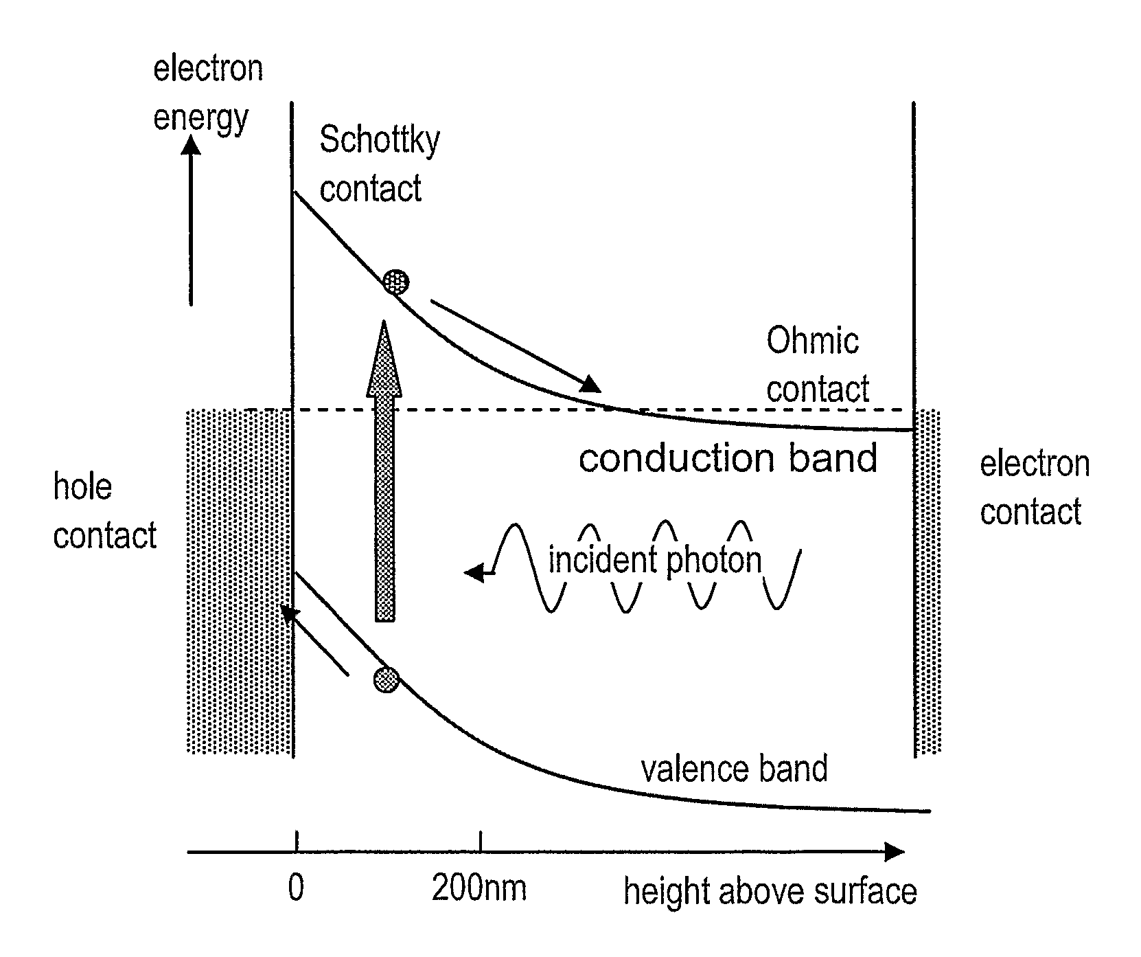
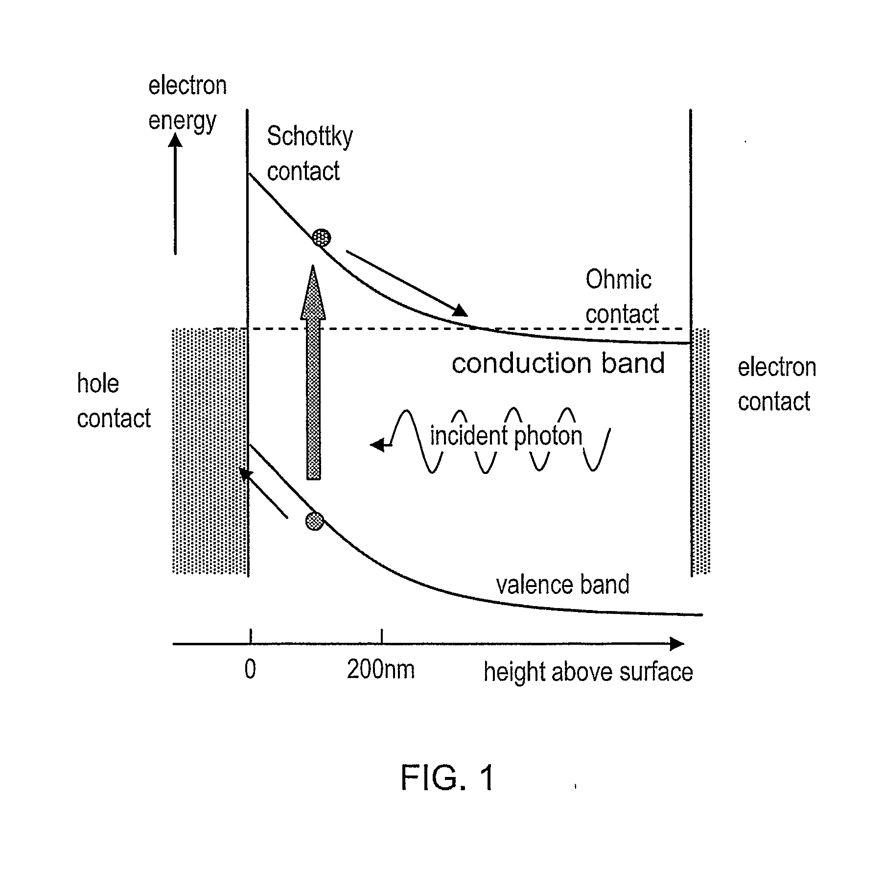
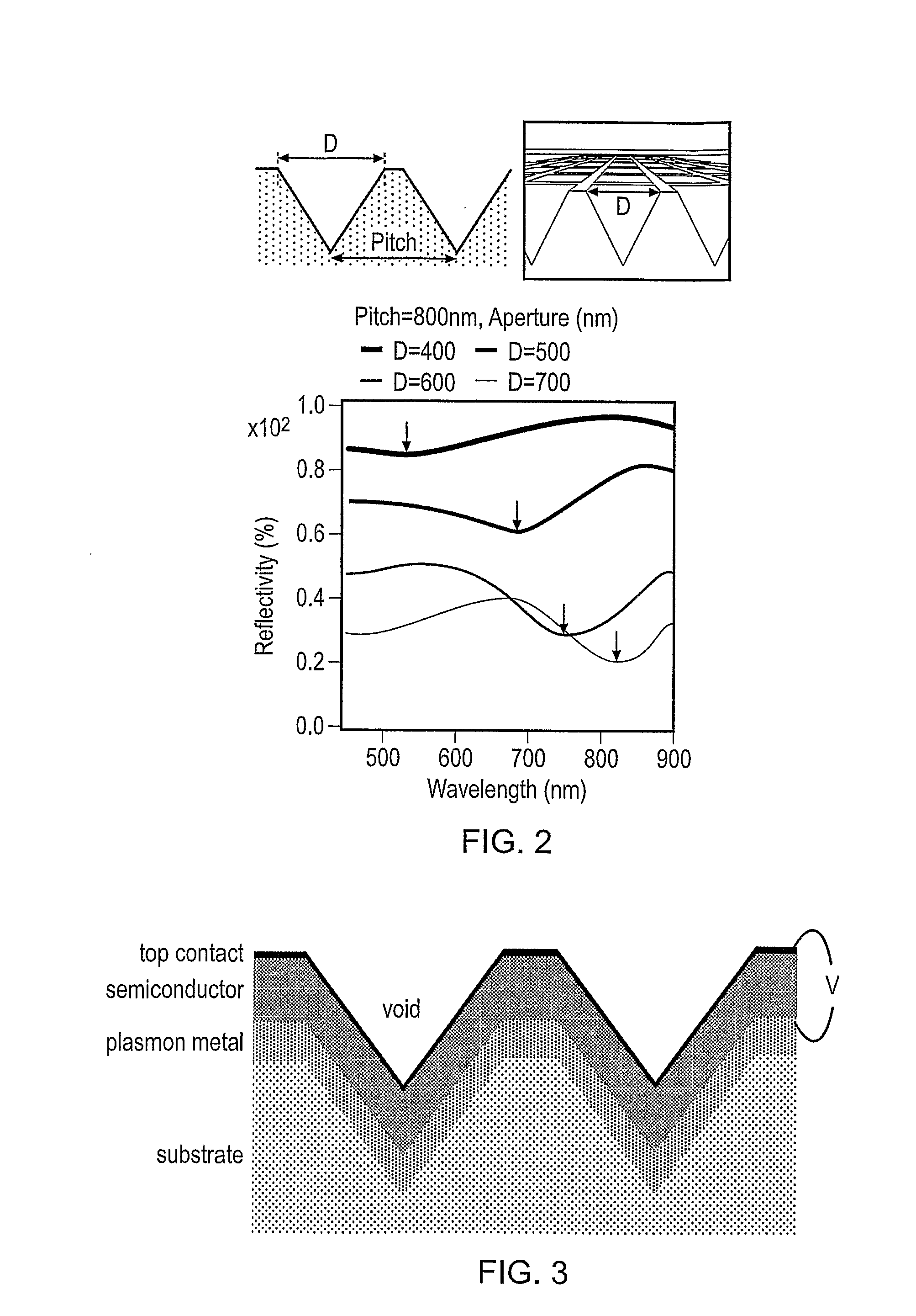
[0023]The novel feature of the solar cell in this patent is the metallic void geometry which is coated with the active absorbing layer embedded in a semiconductor and a top contact. The interface between the doped semiconductor and metal forms a high electric field (Schottky) region (FIG. 1). However normally, because of the interference between incident and reflected light rays, there would be no optical intensity within this high electric field region above a metal. In our structures, the nanostructure plasmon geometry allows strong optical intensity at the surface of the metal, thus generating electron-hole pairs in the place where they can be most easily separated and transported into the contacts.

[0024]Unlike a Grätzel electrochemical cell, this device needs no ion transport layers, but uses the heavily doped as-grown semiconductor to transport electrons to the top contact—this is likely to give better lifetime as ion-transport layers can degrade as often problematic in a batte...


PUM

PropertyMeasurementUnit
depletion lengthaaaaaaaaaa
diameteraaaaaaaaaa

Abstract

A photovoltaic device and a method of making the photovoltaic device. The device includes a metallic surface defining a plurality of voids for confining surface plasmons. The metallic surface is coated with a semiconductor to form a Schottky region at an interface between the metallic surface and the semiconductor within each void.

Description

BACKGROUND OF THE INVENTION[0001]The invention relates to photovoltaic cells. In particular, this invention relates to a plasmon-enhanced photovoltaic cell.[0002]Photovoltaic technology struggles to deliver high efficiency yet cheap modules. Conventional silicon units reach 30% efficiencies and last for over 25 years but are expensive, while organic photovoltaics are having problems both with efficiencies below 10% and sensitivity to oxygen which reduces lifetimes below 5 years. Defects in semiconductors trap carriers reducing efficiencies, but high quality material is expensive to make.SUMMARY OF THE INVENTION[0003]Aspects of the invention are defined in the accompanying claims.[0004]According to an aspect of the invention there is provided a photovoltaic device comprising a metallic surface defining a plurality of voids for confining surface plasmons, wherein the metallic surface is coated with a semiconductor to form a Schottky region at an interface between the metallic surface ...

Claims


Application Information

Patent Timeline
Patent Type & Authority Applications(United States)
IPC IPC(8): H01L31/108H01L31/18H01L31/07
CPCH01L31/03529Y02E10/50H01L31/07
Inventor BAUMBERG, JEREMY JOHNABDELSALAM, MAMDOUTHBARTLETT, PHILIP NIGEL
Owner CAMBRIDGE ENTERPRISE LTD
Why Eureka
Try Eureka