Method of eliminating micro-trenches during spacer etch

a spacer etch and micro-trench technology, applied in the field of integrated circuits, can solve the problems of difficult process, difficult to reduce the size of the device, and the cost of the semiconductor fabrication facility can cost hundreds of millions or even billions of dollars, and achieve the effect of reducing voiding, effective gap filling process, and convenient us

Active Publication Date: 2010-01-14
SEMICON MFG INT (SHANGHAI) CORP +1
View PDF5 Cites 7 Cited by
  • Summary
  • Abstract
  • Description
  • Claims
  • Application Information

AI Technical Summary

Benefits of technology

[0011]Many benefits are achieved by way of the present invention over conventional techniques. For example, the present technique provides an easy to use process that relies upon conventional technology. In some embodiments, an effective gapfill process is provided which reduces voiding within the deposited gapfill layer. For example, the amount of voiding occurring as a result of micro-trenching is greatly reduced. This can improve the device reliability and performance of the semiconductor circuit being formed by providing superior electrical isolation. In addition, lower leakage current and a tighter electrical distribution can also result. Additionally, the method provides a process that is compatible with conventional process technology without substantial modifications to conventional equipment and processes. Depending upon the embodiment, one or more of these benefits may be achieved. These and other benefits will be described in more throughout the present specification and more particularly below.

Problems solved by technology

An IC fabrication facility can cost hundreds of millions, or even billions, of dollars.
Making devices smaller is very challenging, as each process used in IC fabrication has a limit.
Additionally, as devices require faster and faster designs, process limitations exist with conventional processes and materials.
One such example of a process limitation deals with the difficulty of controlling etch selectivity within an ONO spacer etch process.
Micro-trenches can lead to voids and tunnels forming, which can cause moisture or chemicals to be trapped during subsequent processing steps.
This can result in lowered electrical reliability and an increase in the amount of short circuits within the completed circuit.

Method used


Image

  • Method of eliminating micro-trenches during spacer etch
  • Method of eliminating micro-trenches during spacer etch
  • Method of eliminating micro-trenches during spacer etch

Examples


Embodiment Construction

[0025]The present invention is directed to integrated circuits and their processing for the manufacture of semiconductor devices. More particularly, the invention provides a method of semiconductor device formation with reduced void formation and a resulting structure. Merely by way of example, the invention has been applied to the formation of shallow trench isolation (STI) regions. But it would be recognized that the invention has a much broader range of applicability.

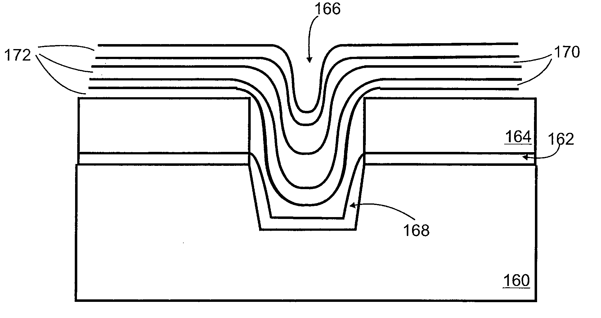
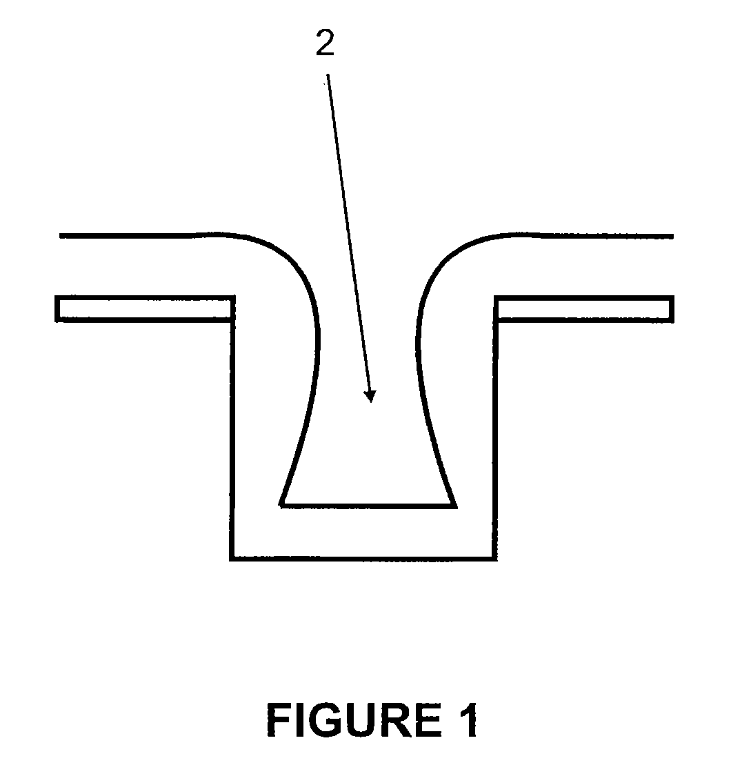
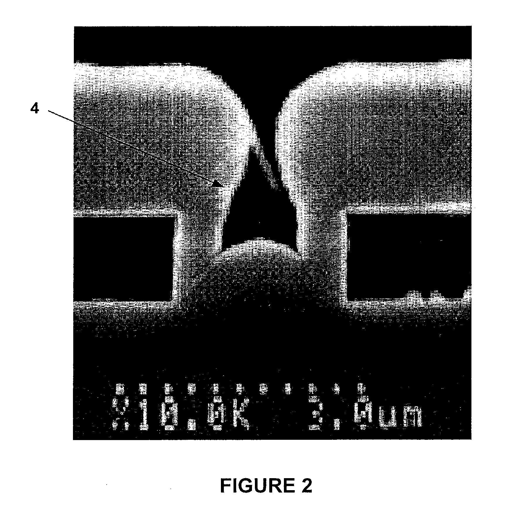
[0026]FIG. 1 is a simplified drawing showing void formation in a conventional trench filling process and FIG. 2 is a SEM image of void formation in a conventional STI process. A deposition process is used to fill the high aspect ratio trenches formed within the substrate. For example, a high aspect ratio trench is a trench where the ratio of the trench depth to the trench width is greater than 5:1. A trench with exemplary dimensions of a trench opening of 12 microns and a depth of 5000 Å can incur a number of problem...


PUM


Abstract

A method of forming a semiconductor structure is provided. The method includes providing a semiconductor substrate with a substrate region. The method also includes forming a pad oxide layer overlying the substrate region. The method additionally includes forming a stop layer overlying the pad oxide layer. Furthermore, the method includes patterning the stop layer and the pad oxide layer to expose a portion of the substrate region. In addition, the method includes forming a trench within an exposed portion of the substrate region, the trench having sidewalls and a bottom and a height. Also, the method includes depositing alternating layers of oxide and silicon nitride to at least fill the trench, the oxide being deposited by an HDP-CVD process. The method additionally includes performing a planarization process to remove a portion of the silicon nitride and oxide layers. In addition, the method includes removing the pad oxide and stop layers.

Description

CROSS-REFERENCE TO RELATED APPLICATIONS[0001]This application claims priority to Chinese Patent Application No. 200810040371.7, filed Jul. 8, 2008, commonly assigned, and incorporated herein by reference for all purposes.BACKGROUND OF THE INVENTION[0002]The present invention is directed to integrated circuits and their processing for the manufacture of semiconductor devices. More particularly, the invention provides a method of semiconductor device formation with reduced void formation and a resulting structure. Merely by way of example, the invention has been applied to the formation of shallow trench isolation (STI) regions. But it would be recognized that the invention has a much broader range of applicability.[0003]Integrated circuits or “ICs” have evolved from a handful of interconnected devices fabricated on a single chip of silicon to millions of devices. Current ICs provide performance and complexity far beyond what was originally imagined. In order to achieve improvements i...

Claims


Application Information

Patent Timeline
Patent Type & Authority Applications(United States)
IPC IPC(8): H01L29/00H01L21/76
CPCH01L21/76224
Inventor ANG, TING CHEONG
Owner SEMICON MFG INT (SHANGHAI) CORP
Why Eureka
Try Eureka