High band gap contact layer in inverted metamorphic multijunction solar cells

a solar cell and contact layer technology, applied in the field of solar cell semiconductor devices and multijunction solar cells, can solve the problems of increasing the cost of solar cells, affecting the performance of solar cells, and presenting a number of practical difficulties

Inactive Publication Date: 2010-01-21
SOLAERO TECH CORP
View PDF91 Cites 73 Cited by
  • Summary
  • Abstract
  • Description
  • Claims
  • Application Information

AI Technical Summary

Benefits of technology

[0027]A multijunction solar cell comprising: a first solar subcell having a first band gap; a second solar subcell disposed over the first solar subcell having a second band gap smaller than the first band gap; a graded interlayer disposed over the second subcell having a third band gap greater than the second...

Problems solved by technology

While significant progress has been made in this area, the requirement for solar cells to meet the needs of more sophisticated applications has not kept pace with demand.
The structures described in such reference present a number of practical difficulties relating to the appropriate choice of materials and fabrication steps, for a number of different layers of the cell.
One issue in all types of cells has been the dark current in the photovoltaic cell.
Such approach adds processing steps, and also requires that the sheet resistance of the layers below the junction ha...

Method used


Image

  • High band gap contact layer in inverted metamorphic multijunction solar cells
  • High band gap contact layer in inverted metamorphic multijunction solar cells
  • High band gap contact layer in inverted metamorphic multijunction solar cells

Examples


second embodiment

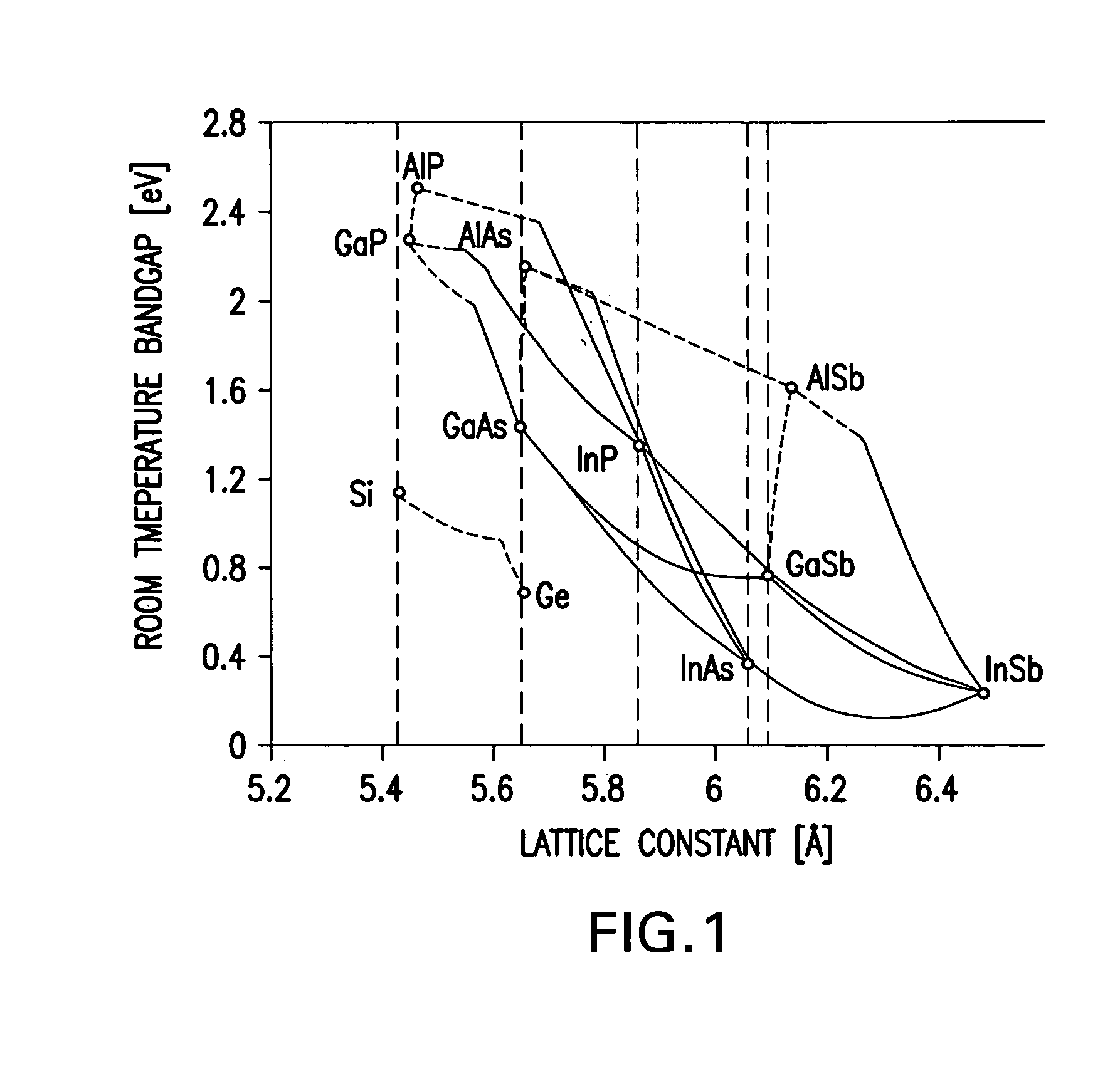
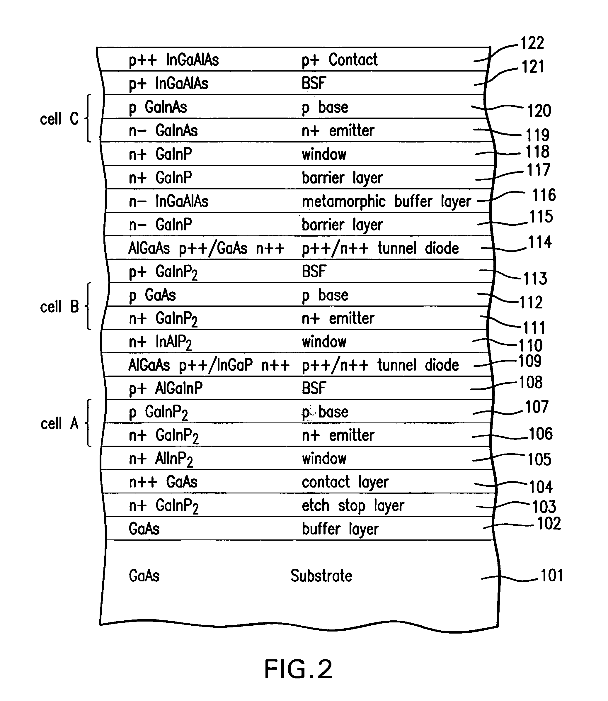
[0074]Although the preferred embodiment of the present invention utilizes a plurality of layers of InGaAlAs for the metamorphic layer 116 for reasons of manufacturability and radiation transparency, other embodiments of the present invention may utilize different material systems to achieve a change in lattice constant from subcell B to subcell C. Thus, the system of Wanlass using compositionally graded InGaP is the present invention. Other embodiments of the present invention may utilize continuously graded, as opposed to step graded, materials. More generally, the graded interlayer may be composed of any of the As, P, N, Sb based III-V compound semiconductors subject to the constraints of having the in-plane lattice parameter greater or equal to that of the second solar cell and less than or equal to that of the third solar cell, and having a bandgap energy greater than that of the second solar cell.

[0075]In another embodiment of the present invention, an optional second barrier l...

first embodiment

[0098]FIG. 14A is a cross-sectional view of the solar cell of FIG. 12 after the next process step in the present invention in which the surrogate substrate 125 is appropriately thinned to a relatively thin layer 125a, by grinding, lapping, or etching.

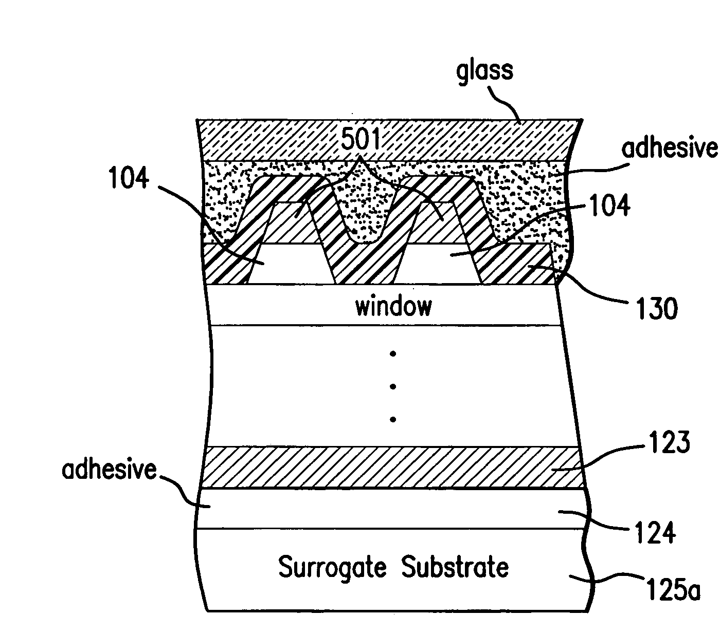
[0099]FIG. 14B is a cross-sectional view of the solar cell of FIG. 14A after the next process step in a second embodiment of the present invention in which a cover glass is secured to the top of the cell by an adhesive.

third embodiment

[0100]FIG. 15 is a cross-sectional view of the solar cell of FIG. 14B after the next process step in the present invention in which a cover glass is secured to the top of the cell and the surrogate substrate 125 is entirely removed, leaving only the metal contact layer 123 which forms the backside contact of the solar cell. The surrogate substrate may be reused in subsequent wafer processing operations.

[0101]FIG. 16 is a graph of a doping profile in the emitter and base layers in one or more subcells of the inverted metamorphic multijunction solar cell of the present invention. The various doping profiles within the scope of the present invention, and the advantages of such doping profiles are more particularly described in copending U.S. patent application Ser. No. 11 / 956,069 filed Dec. 13, 2007, herein incorporated by reference. The doping profiles depicted herein are merely illustrative, and other more complex profiles may be utilized as would be apparent to those skilled in the ...


PUM


Abstract

A method of forming a multijunction solar cell including an upper subcell, a middle subcell, and a lower subcell by providing a substrate for the epitaxial growth of semiconductor material; forming a first solar subcell on the substrate having a first band gap; forming a second solar subcell over the first solar subcell having a second band gap smaller than the first band gap; forming a graded interlayer over the second subcell, the graded interlayer having a third band gap greater than the second band gap; forming a third solar subcell over the graded interlayer having a fourth band gap smaller than the second band gap such that the third subcell is lattice mismatched with respect to the second subcell; and forming a contact layer over the third subcell having a fifth band gap greater than at least the magnitude of the second band gap.

Description

REFERENCE TO RELATED APPLICATIONS[0001]This application is related to co-pending U.S. patent application Ser. No. 12 / 123,864 filed May 20, 2008.[0002]This application is related to co-pending U.S. patent application Ser. No. 12 / 102,550, filed Apr. 14, 2008.[0003]This application is related to co-pending U.S. patent application Ser. No. 12 / 047,842, and U.S. Ser. No. 12 / 047,944, filed Mar. 13, 2008.[0004]This application is related to co-pending U.S. patent application Ser. No. 12 / 023,772, filed Jan. 31, 2008.[0005]This application is related to co-pending U.S. patent application Ser. No. 11 / 956,069, filed Dec. 13, 2007.[0006]This application is also related to co-pending U.S. patent application Ser. Nos. 11 / 860,142 and 11 / 860,183 filed Sep. 24, 2007.[0007]This application is also related to co-pending U.S. patent application Ser. No. 11 / 836,402 filed Aug. 8, 2007.[0008]This application is also related to co-pending U.S. patent application Ser. No. 11 / 616,596 filed Dec. 27, 2006.[0009...

Claims


Application Information

Patent Timeline
IPC IPC(8): H01L31/00H01L21/306H01L21/02
CPCH01L21/02395H01L21/02433H01L21/02463Y02E10/544H01L31/06875H01L31/078H01L31/1844H01L21/02538Y02P70/50
Inventor VARGHESE, TANSENSTAN, MARK A.CORNFELD, ARTHURNEWMAN, FREDGRAY, ALLEN A.
Owner SOLAERO TECH CORP
Why Eureka
Try Eureka