Light-emitting diode device and method for fabricating the same

a technology of led devices and light-emitting diodes, which is applied in the direction of semiconductor/solid-state device manufacturing, semiconductor devices, electrical apparatus, etc., can solve the problems of long life, low power consumption, and high cost of led devices above three-in-one white ligh

Inactive Publication Date: 2010-01-21
SEMILEDS OPTOELECTRONICS CO LTD +1
View PDF7 Cites 31 Cited by
  • Summary
  • Abstract
  • Description
  • Claims
  • Application Information

AI Technical Summary

Benefits of technology

[0009]An embodiment of a method for fabricating semiconductor devise comprises providing a semiconductor wafer comprising a plurality of cavities and a plurality of light-emitting diode chips in the corresponding cavities. The plurality of cavities of the semiconductor wafer is capped with a lens plate, in which the lens plate comprises a plurality of molded lenses, a plurality of molded fluorescent layers under the corresponding molded lenses and the molded fluorescent layer faces the and faces the corresponding light-emitting diode chips, and a glass wafer interposed between the plurality of molded fluorescent layers and the plurality of molded lenses. The bottom surface of the semiconductor wafer is etched to form a plurality of notches between the adjacent cavities to form individual semiconductor substrates. The lens plate is cut from the plurality of notches to form individual lens modules on the corresponding semiconductor substrates.
[0010]Another embodiment of a method for fabricating semiconductor devises comprises providing a semiconductor wafer comprising a plurality of cavities and a plurality of light-emitting diode chips in the corresponding cavities. Each cavity of the semiconductor wafer is capped with a lens module, in which each lens module comprises a molded lens and a molded fluorescent layer thereunder and the molded fluorescent layer faces the light-emitting diode chip. The semiconductor wafer between the adjacent cavities is cut to form individual semiconductor substrates with the corresponding lens module.

Problems solved by technology

Advantages of LED devices compared with traditional lamps are lower power consumption and longer lifespan.
However, the above three-in-one white light LED device is expensive because it requires three LED chips for different emitted lights.
However, poor uniformity of the filled epoxy resin reduces the light-emitting properties of the LED devices.
However, the coating rate of the epoxy resin layer is slow and it is also difficult to control the uniformity of the epoxy resin layer.
However, the coating rate of the epoxy resin layer is also slow and the manufacturing cost is high.

Method used


Image

  • Light-emitting diode device and method for fabricating the same
  • Light-emitting diode device and method for fabricating the same
  • Light-emitting diode device and method for fabricating the same

Examples


Embodiment Construction

[0017]The following description is of the best-contemplated mode of carrying out the invention. This description is provided for the purpose of illustrating the general principles of the invention and should not be taken in a limiting sense. The scope of the invention is best determined by reference to the appended claims.

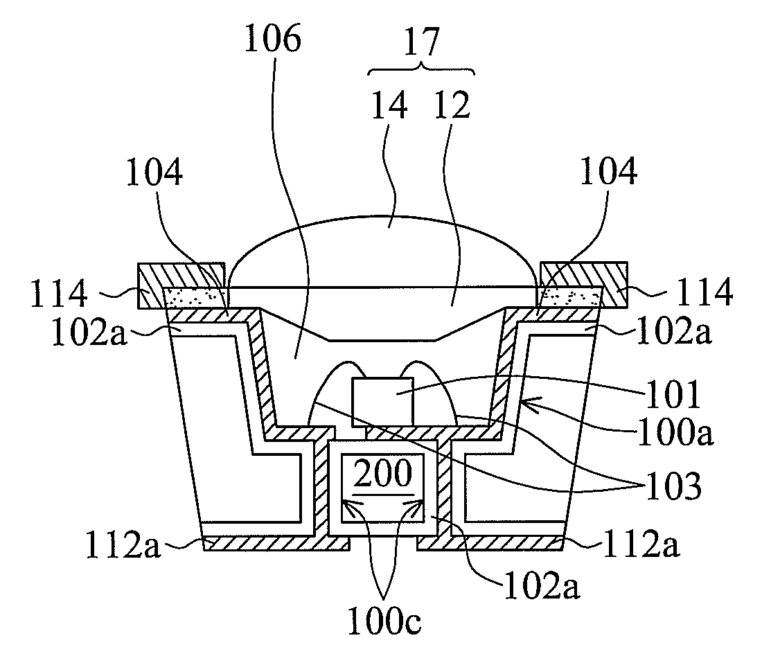
[0018]FIGS. 3D, 4D and 5C, are cross sections of various exemplary embodiments of LED devices according to the invention, respectively. Elements in FIGS. 4D and 5C that are the same as those in FIG. 3D are labeled with the same reference numbers as in FIG. 3D and are not described again for brevity. Referring to FIG. 3D, the LED device comprises a semiconductor substrate 200, such as a silicon substrate or other semiconductor substrates well known in the art, having a cavity 100a. The semiconductor substrate 200 may contain a variety of elements, including, for example, transistors, resistors, and other semiconductor elements well known in the art. In order to simp...


PUM


Abstract

A semiconductor device is disclosed. The semiconductor device comprises a light-emitting diode chip disposed in a cavity of a semiconductor substrate. At least two isolated outer wiring layers are disposed on the bottom surface of the semiconductor substrate and are electrically connected to the light-emitting diode chip, serving as input terminals. A lens module is adhered to the top surface of the semiconductor substrate to cap the cavity, in which the lens module comprises a molded lens and a molded fluorescent layer thereunder and the molded fluorescent layer faces the light-emitting diode chip. A method for fabricating the semiconductor devices is also disclosed.

Description

BACKGROUND OF THE INVENTION[0001]1. Field of the Invention[0002]The invention relates to a light-emitting diode (LED) device and more particularly to LED devices with a lens module having a fluorescent material and methods for fabricating the same.[0003]2. Description of the Related Art[0004]Light-emitting diode (LED) devices are solid-state light sources and have been known for years. The LED devices are based on the recombination of electron-hole pairs in a pn-junction in a semiconductor material which is forward-biased. Advantages of LED devices compared with traditional lamps are lower power consumption and longer lifespan. In particular, because white light LED devices have high color rendering index (CRI), it has become one of the most popular illuminating devices used.[0005]A white light LED device can be obtained by mixing red, green, and blue lights using a combination of a red light LED chip (or die), a green light LED chip, and a blue light LED chip to form the white ligh...

Claims


Application Information

Patent Timeline
Patent Type & Authority Applications(United States)
IPC IPC(8): H01L33/00
CPCH01L33/46H01L33/486H01L33/507H01L33/58H01L33/62H01L2224/48091H01L2924/10253H01L2924/00012H01L2924/00H01L2924/00014
Inventor LIN, TZU-HANWENG, JUI-PINGSHIUNG, SHIN-CHANG
Owner SEMILEDS OPTOELECTRONICS CO LTD
Why Eureka
Try Eureka