Power semiconductor device

a technology of power semiconductor and semiconductor device, which is applied in the direction of printed circuit, sustainable manufacturing/processing, final product manufacturing, etc., can solve the problems of difficult to reduce the size of the power semiconductor device, low productivity, and long manufacturing time, and achieve high yield, excellent productivity, and reduce defects

Active Publication Date: 2010-01-21
MITSUBISHI ELECTRIC CORP
View PDF4 Cites 82 Cited by
  • Summary
  • Abstract
  • Description
  • Claims
  • Application Information

AI Technical Summary

Benefits of technology

[0013]The present invention has been made to solve the above problems. The object of the present invention is to provide a power semiconductor device sealed with transfer molding resin, which is capable of, even if external wiring capable of applying a large current is connected to a main terminal connected to a main circuit of the power semiconductor device, reducing defects that occur at the main terminal area due to the connection with the external wiring. The provided power semiconductor device is also high in yield, excellent in terms of productivity, and highly reliable.
[0014]A power semiconductor device according to the present invention includes a circuit substrate including a metal heat sink and including a high thermal conductive insulation layer joined to one surface of the metal heat sink and including wiring patterns provided on a surface of the high thermal conductive insulation layer, which surface is opposite to a surface, of the high thermal conductive insulation layer, joined to the metal heat sink; power semiconductor elements joined to the wiring patterns; cylindrical external terminal communication sections joined to the wiring patterns; and wiring means for establishing conduction between the power semiconductor elements, between the wiring patterns, and between the power semiconductor elements and the wiring patterns. The circuit substrate, the power semiconductor elements, the cylindrical external terminal communication sections, and the wiring means are all sealed with transfer molding resin. The cylindrical external terminal communication sections are joined to the wiring patterns so as to be substantially perpendicular to the wiring patterns, such that a plurality of cylindrical external terminal communication sections among the cylindrical external terminal communication sections are two-dimensionally arranged on each of wiring patterns that act as main circuits. Holes of the cylindrical external terminal communication sections, to which external terminals are insertable and connectable, are exposed at a top surface of the transfer molding resin. Since the power semiconductor device according to the present invention has the above configuration, the stress, which occurs due to the connection of the external terminals to the cylindrical external terminal communication sections, can be dispersed and reduced, and defects at the cylindrical external terminal communication sections can be prevented.
[0015]Another power semiconductor device according to the present invention includes a plurality of AC-side cylindrical external terminal communication sections that are arranged two-dimensionally on wiring patterns, a plurality of DC-side cylindrical external terminal communication sections that are arranged two-dimensionally on the wiring patterns, and power semiconductor elements electrically conductive with the plurality of AC-side cylindrical external terminal communication sections and the plurality of DC-side cylindrical external terminal communication sections. The plurality of AC-side cylindrical external terminal communication sections, the plurality of DC-side cylindrical external terminal communication sections, and the power semiconductor elements are all sealed with transfer molding resin. The AC-side and DC-side cylindrical external terminal communication sections have holes formed at a top surface of the transfer molding resin. The AC-side cylindrical external terminal communication sections are connected to an AC-side external terminal. The DC-side cylindrical external terminal communication sections are connected to a DC-side wiring substrate. The AC-side cylindrical external terminal communication sections are connected to a connection between a negative electrode of a positive-electrode-side power semiconductor element from among the power semiconductor elements and a positive electrode of a negative-electrode-side power semiconductor element from among the power semiconductor elements. A plurality of connecting pins to be connected to the AC-side cylindrical external terminal communication sections are two-dimensionally provided in a plate portion of the AC-side external terminal. The DC-side cylindrical external terminal communication sections include a plurality of positive-electrode-side cylindrical external terminal communication sections and a plurality of negative-electrode-side cylindrical external terminal communication sections. The positive-electrode-side cylindrical external terminal communication sections are connected to a positive electrode of the positive-electrode-side power semiconductor element, and the negative-electrode-side cylindrical external terminal communication sections are connected to a negative electrode of the negative-electrode-side power semiconductor element. The DC-side wiring substrate is formed by integrating a positive-electrode-side wiring board and a negative-electrode-side wiring board with an insulation layer interposed therebetween, the positive-electrode-side wiring board being connected to the positive-electrode-side cylindrical external terminal communication sections via connecting pins, and the negative-electrode-side wiring board being connected to the negative-electrode-side cylindrical external terminal communication sections via connecting pins. A plurality of connecting pins to be connected to the DC-side cylindrical external terminal communication sections are provided two-dimensionally in a plate portion of the DC-side wiring substrate formed by said integrating. Since this other power semiconductor device according to the present invention has the above configuration, the stress, which occurs due to the connection of the external terminals to the cylindrical external terminal communication sections, can be dispersed and reduced, and defects at the cylindrical external terminal communication sections can be prevented. In addition, circuit inductance can be reduced, and surge voltage that occurs when a large current supply is cut off can be suppressed.

Problems solved by technology

Thus, there are a large number of manufacturing processes, causing a prolonged manufacturing time.
Accordingly, there is a problem of low productivity.
Accordingly, there is a problem that it is difficult to reduce the size of the power semiconductor device.
In addition, since a bending process is performed on the lead frames that are used as the external terminals, there is a limitation regarding the thickness thereof.
Thus, there is a problem that an increase in the current is limited in the power semiconductor device.
Due to this stress, there is a problem that defects occur at the main terminal area, for example, a gap occurs at a joint surface between the outer side surface of the main terminal and the transfer molding resin, or fine cracks occur in the transfer molding resin.
This causes problems of low yield, low productivity, and low reliability of the power semiconductor device.
These problems are more prominent when the connection to the external wiring is formed by thread connection.
Further, since a large current is applied, even if a cable is used for external wiring to be connected to the main terminal, the cable used herein is highly rigid.
Accordingly, the same problems occur.

Method used


Image

  • Power semiconductor device
  • Power semiconductor device
  • Power semiconductor device

Examples


first embodiment

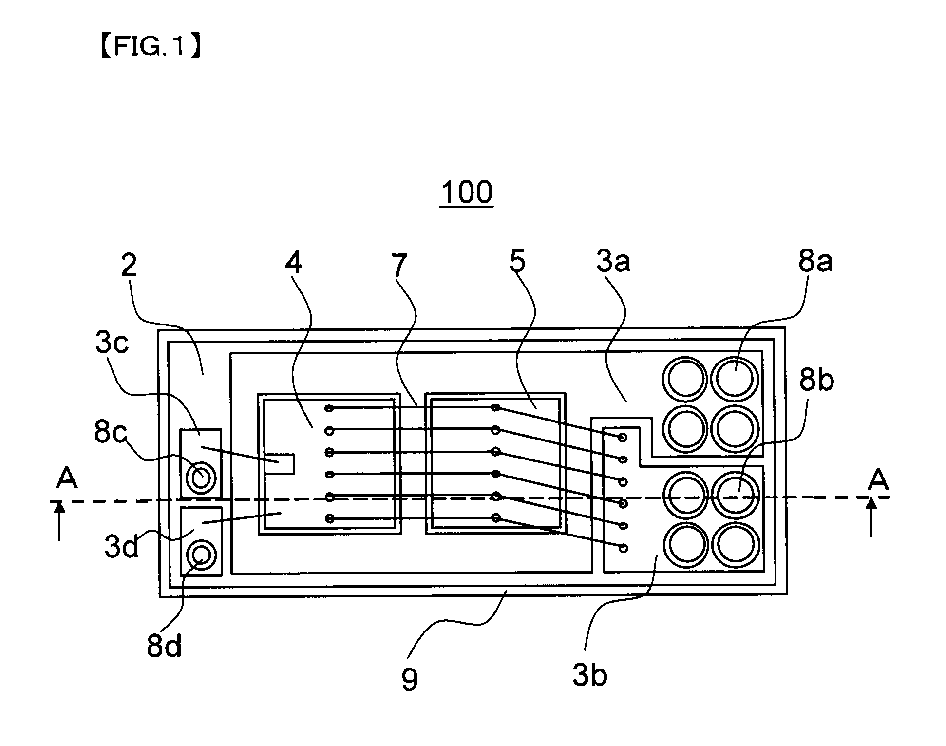
[0030]FIG. 1 is a schematic plane view showing that transfer molding resin on a circuit substrate of a power semiconductor device according to the first embodiment of the present invention, is removed.

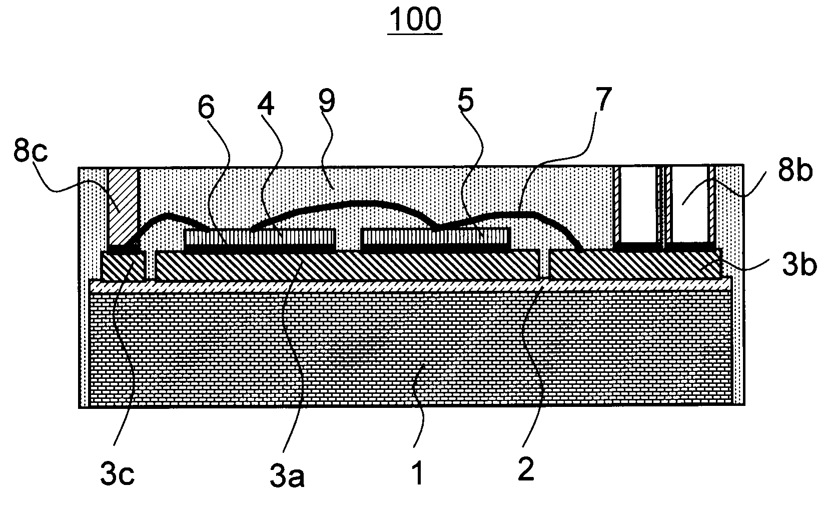
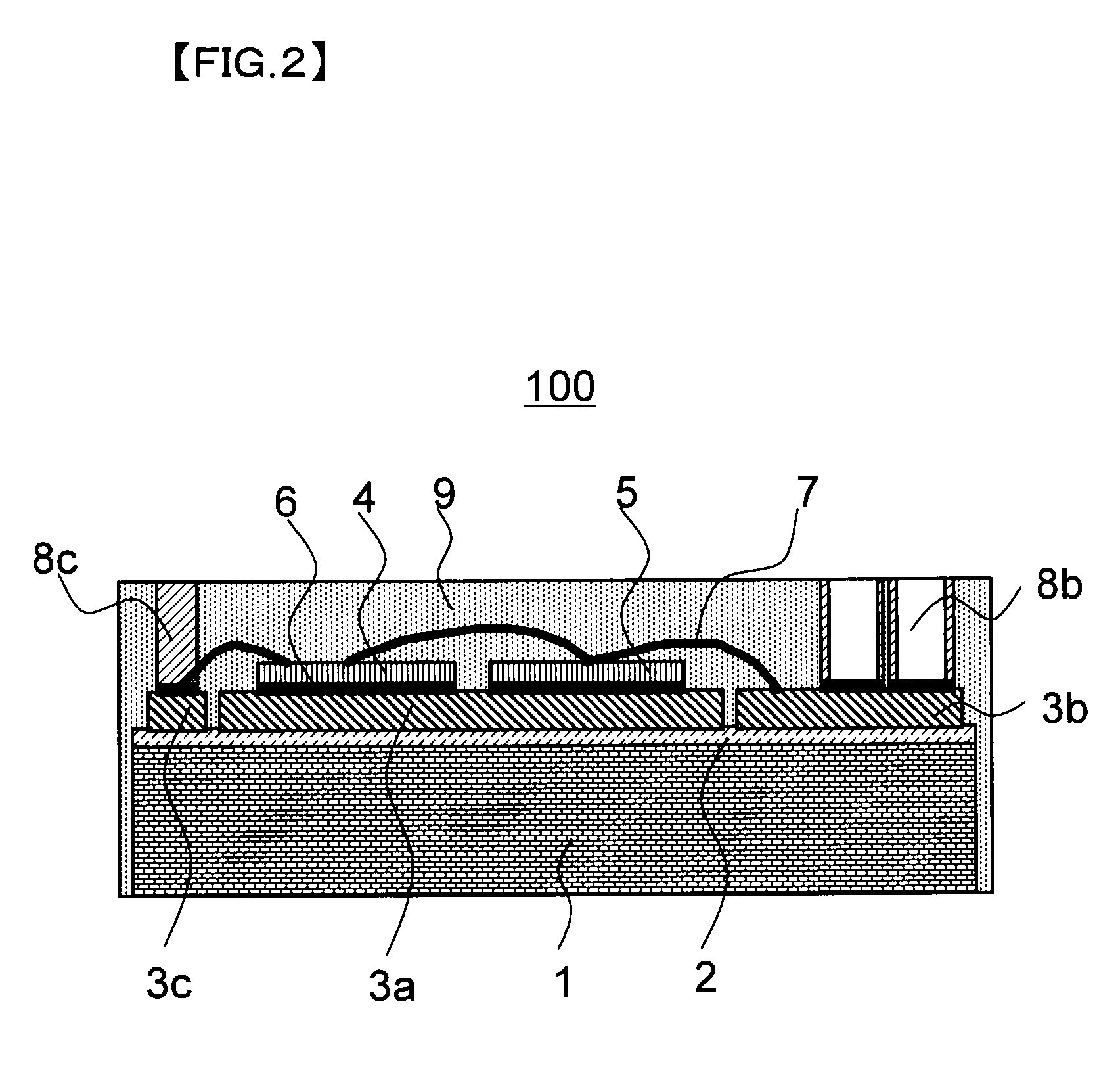
[0031]FIG. 2 is a schematic cross sectional view of the power semiconductor device shown in FIG. 1, which is cut along a line A-A indicated in FIG. 1 when the transfer molding resin is present on the circuit substrate.

[0032]As shown in FIGS. 1 and 2, in a power semiconductor device 100 of the present embodiment, a metal circuit substrate is used, which is formed such that: a resin insulation layer 2 is provided on one surface of a metal heat sink 1; and wiring patterns are provided on a surface of the resin insulation layer 2, which surface is opposite to a surface, of the resin insulation layer 2, joined to the metal heat sink 1. An IGBT 4 and a diode 5 connected in antiparallel with the IGBT 4, which are power semiconductor elements, are mounted on one of the wiring patterns. These p...

second embodiment

[0081]FIG. 4 is a schematic top view of a power semiconductor device according to the second embodiment of the present invention.

[0082]FIG. 5 is a schematic cross sectional view of the power semiconductor device shown in FIG. 4, which is cut along a line B-B indicated in FIG. 4.

[0083]In the present embodiment, a surface of the transfer molding resin 9, at which holes of cylindrical external terminal communication sections of the power semiconductor device are present, is referred to as a top surface.

[0084]As shown in FIGS. 4 and 5, a power semiconductor device 200 of the present embodiment is the same as the power semiconductor device 100 of the first embodiment except that in the present embodiment, external terminals 20 each provided with connecting pins 21 are connected to the cylindrical external terminal communication sections of the power semiconductor device 100 of the first embodiment. One external terminal connecting pin 21 is inserted into the cylindrical external terminal...

third embodiment

[0099]FIG. 7A is a schematic top view showing an external terminal 26 having four connecting pins to be connected to the cylindrical external terminal communication sections of each main circuit of a power semiconductor device according to the third embodiment of the present invention. FIG. 7B is a schematic cross-sectional view which is cut along a line D-D indicated in the schematic top view of FIG. 7A.

[0100]Here, a surface of the plate portion 22 of the external terminal 26, which is the opposite surface to a surface having connecting pins 21 protruding therefrom, is referred to as a top surface.

[0101]The power semiconductor device of the present embodiment (not shown) is the same as the power semiconductor device 200 of the second embodiment except that external terminals 26, each of which has four connecting pins 21 and in each of which the plate portion 22 and the connecting pins 21 are integrated, are used.

[0102]As shown in FIGS. 7A and 7B, in each external terminal 26 of the...


PUM


Abstract

A power semiconductor device includes power semiconductor elements joined to wiring patterns of a circuit substrate, cylindrical external terminal communication sections, and wiring means for forming electrical connection between, for example, the power semiconductor elements and the cylindrical external terminal communication sections. The power semiconductor elements, the cylindrical external terminal communication sections, and the wiring means are sealed with transfer molding resin. The cylindrical external terminal communication sections are arranged on the wiring patterns so as to be substantially perpendicular to the wiring patterns, such that external terminals are insertable and connectable to the cylindrical external terminal communication sections, and such that a plurality of cylindrical external terminal communication sections among the cylindrical external terminal communication sections are arranged two-dimensionally on each of wiring patterns that act as main circuits.

Description

BACKGROUND OF THE INVENTION[0001]1. Field of the Invention[0002]The present invention relates to a resin-sealed power semiconductor device, formed by transfer molding, which is excellent in terms of productivity. The present invention particularly relates to a resin-sealed power semiconductor device, formed by transfer molding, which is small in size, realizes operation with a large current, and is highly reliable.[0003]2. Description of the Background Art[0004]A power semiconductor device capable of operating with a large current and a high voltage, which is able to efficiently discharge heat, which is generated by the operation of the power semiconductor device, to the outside of the power semiconductor device, is the one that is formed such that: power semiconductor elements are mounted on a substrate that includes a metal plate acting as a heat sink and a wiring pattern formed above the metal plate, the substrate including a ceramic plate interposed as an insulation layer betwee...

Claims


Application Information

Patent Timeline
Patent Type & Authority Applications(United States)
IPC IPC(8): H01L23/52H01L23/28H01L23/48
CPCH01L23/3121H01L24/28H01L24/29H01L24/45H01L24/48H01L24/49H01L25/072H01L25/162H01L2224/45124H01L2224/48091H01L2224/48137H01L2224/48227H01L2224/48472H01L2224/48699H01L2224/4911H01L2224/49111H01L2224/49171H01L2224/49175H01L2224/73265H01L2924/01004H01L2924/01005H01L2924/01012H01L2924/01013H01L2924/01014H01L2924/01015H01L2924/0102H01L2924/01028H01L2924/01029H01L2924/01061H01L2924/01075H01L2924/01078H01L2924/01082H01L2924/014H01L2924/10253H01L2924/10272H01L2924/13055H01L2924/13091H01L2924/19043H01L2924/30107H05K3/284H05K3/32H05K2201/1031H05K2201/10333H05K2201/10962H01L2224/32225H01L2924/01006H01L2924/01033H01L2924/1815H01L2924/12032H01L2924/1305H01L2924/00014H01L2924/00H01L2924/00012H01L2924/3512H01L2224/48139H01L2224/45015H01L2924/15787H01L2224/0603H01L2924/181H01L24/73H01L2224/05553Y02P70/50
Inventor OI, TAKESHIOKA, SEIJIOBIRAKI, YOSHIKOUSUI, OSAMUNAKAYAMA, YASUSHI
Owner MITSUBISHI ELECTRIC CORP
Why Eureka
Try Eureka