Light Emitting Device and Electronic Device

Inactive Publication Date: 2010-01-21
SEMICON ENERGY LAB CO LTD
View PDF69 Cites 66 Cited by
  • Summary
  • Abstract
  • Description
  • Claims
  • Application Information

AI Technical Summary

Benefits of technology

[0016]A light emitting element is sealed between the first structure body in which a fibrous body is impregnated with an organic resin and the second structure body in which a fibrous body is impregnated with an organic resin, whereby a

Problems solved by technology

However, when a light emitting device is thinned, a light emitting device, which is formed such that a layer including a semico

Method used


Image

  • Light Emitting Device and Electronic Device
  • Light Emitting Device and Electronic Device
  • Light Emitting Device and Electronic Device

Examples


embodiment 1

[0038]In this embodiment, an example of a light emitting device which is one embodiment of the present invention will be described in detail with reference to FIGS. 1A and 1B.

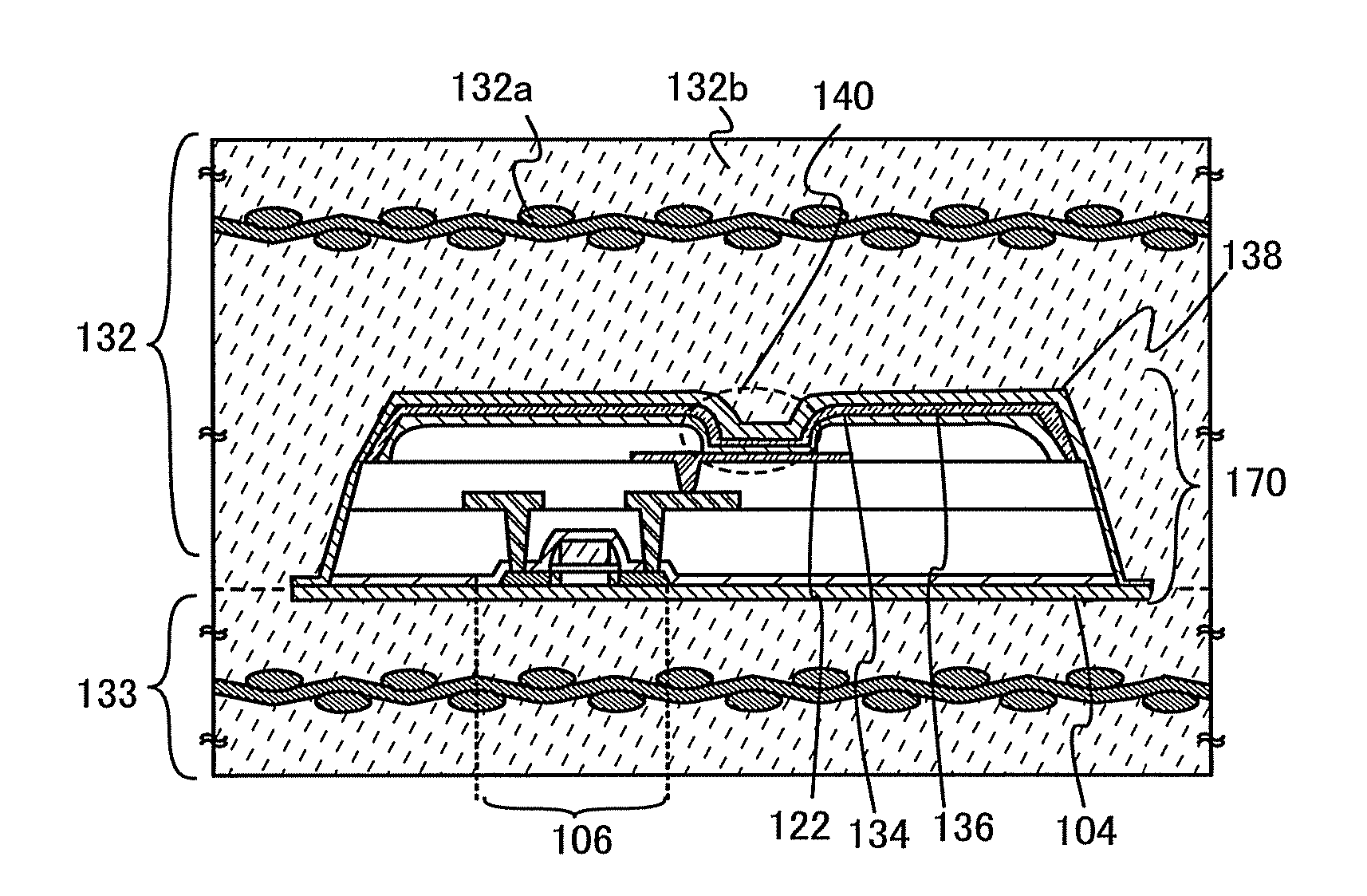
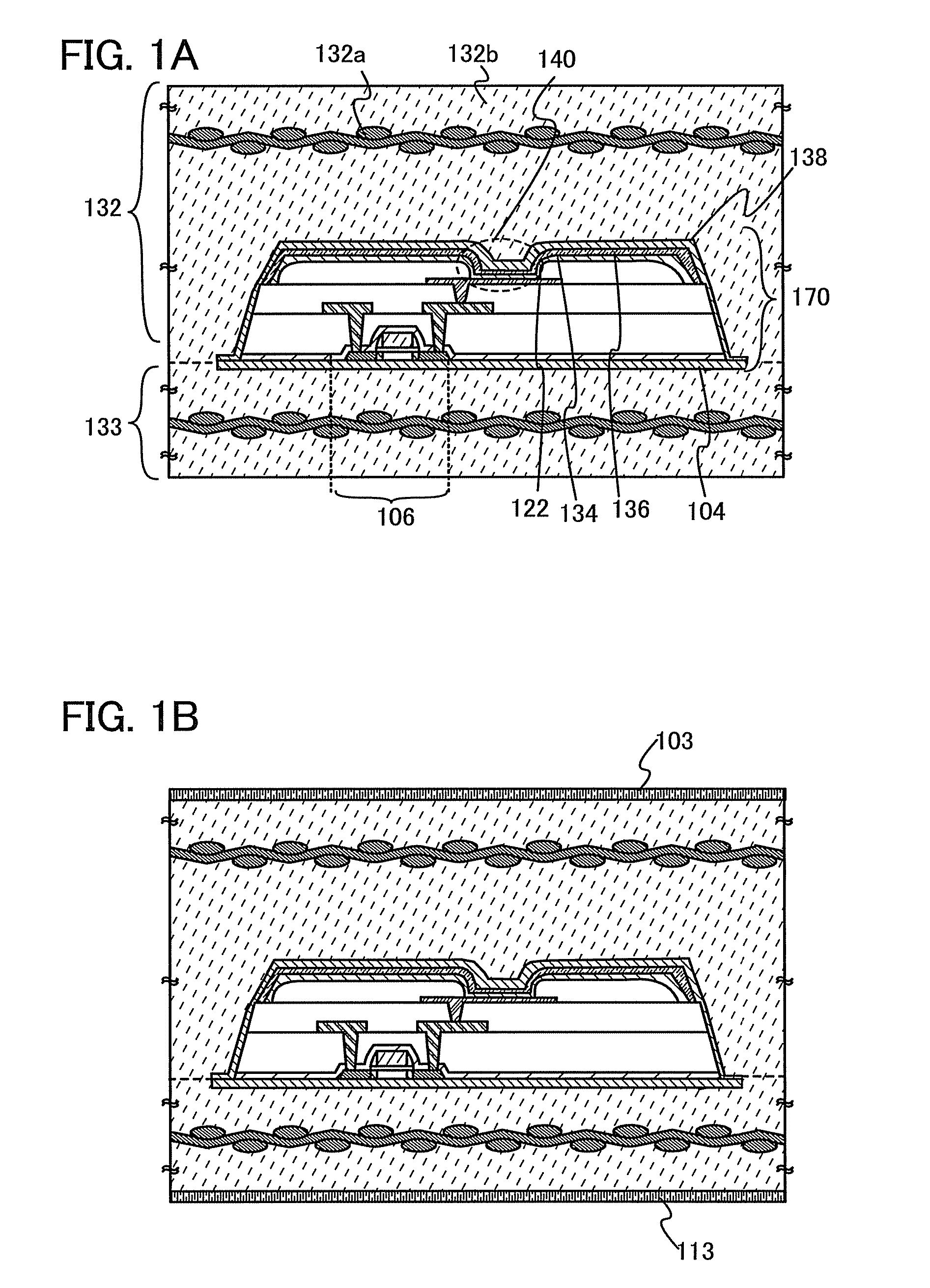
[0039]A display portion of a light emitting device of this embodiment is illustrated in FIGS. 1A and 1B. The light emitting device of this embodiment illustrated in FIG. 1A has an element portion 170 sealed between a first structure body 132 and a second structure body 133. In addition, an insulating layer 104 and an insulating layer 138 are formed between the element portion 170 and the second structure body 133 and between the element portion 170 and the first structure body 132. The first structure body 132 and the second structure body 133 are each a structure body in which a fibrous body 132a is impregnated with an organic resin 132b. In addition, the first structure body 132 and the second structure body 133 are in contact with each other and fixed to each other in a region where the element portion 170 i...

embodiment 2

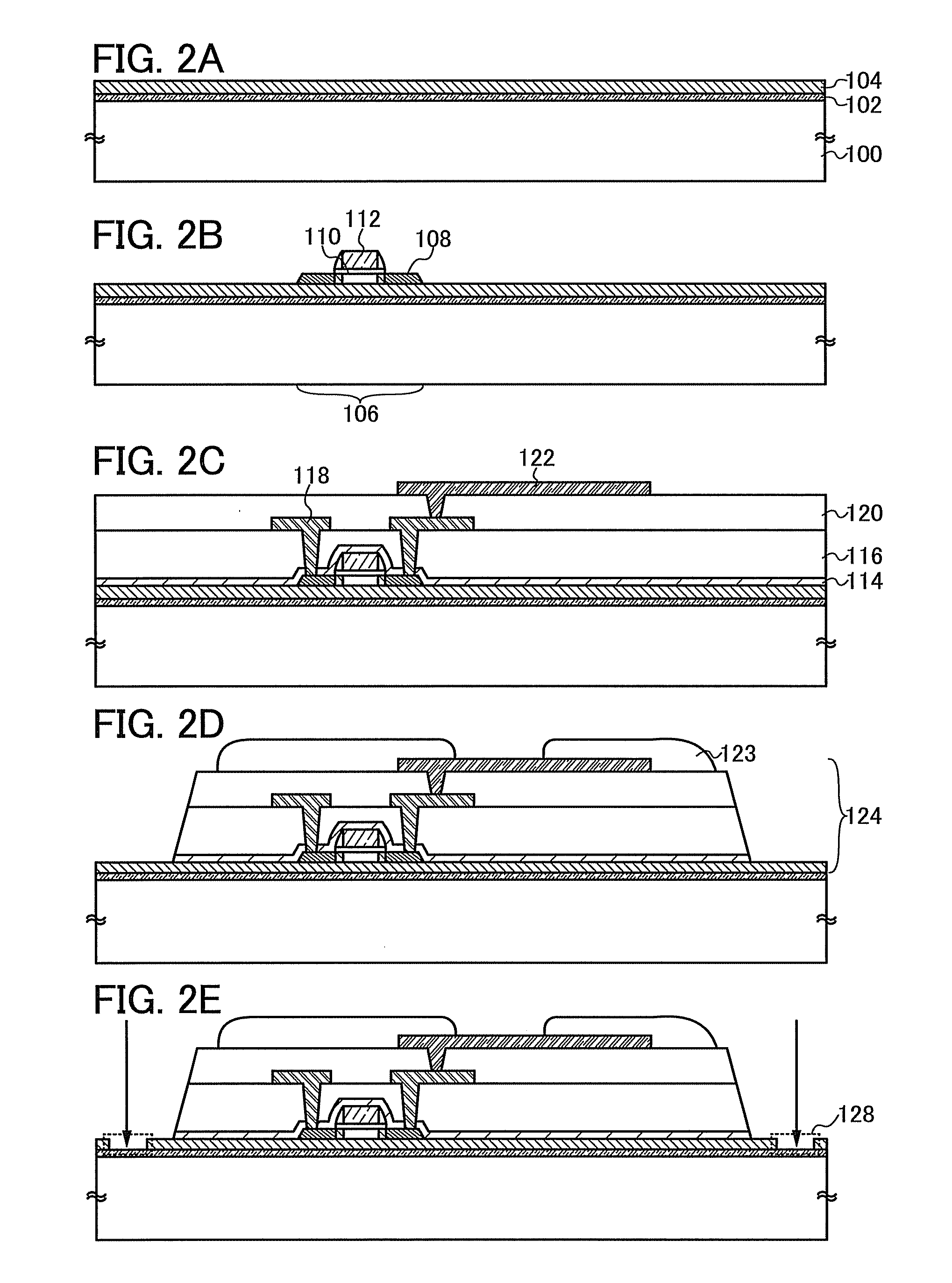
[0058]In this embodiment, an example of a method for manufacturing a light emitting device illustrated in FIG. 1A will be described in detail with reference to FIGS. 2A to 2E, FIGS. 3A to 3C, and FIGS. 4A to 4C.

[0059]First, a separation layer 102 is formed on a surface of a substrate 100; successively, the insulating layer 104 is formed (see FIG. 2A). The separation layer 102 and the insulating layer 104 can be formed in succession. By forming successively, they are not exposed to the air so that impurities can be prevented from being contained therein.

[0060]For the substrate 100, a glass substrate, a quartz substrate, a metal substrate, a stainless steel substrate, or the like may be used. For example, when a rectangular glass substrate with a side of one meter or more is used, productivity can be drastically improved.

[0061]Note that in this process, the case where the separation layer 102 is provided on the entire surface of the substrate 100 is described; however, the separation ...

embodiment 3

[0111]In this embodiment, an example of a method for manufacturing a light emitting device different from that of the aforementioned embodiment will be described with reference to drawings. Note that in this embodiment, a manufacturing process of the light emitting device illustrated in FIG. 1A is described as an example.

[0112]First, the separation layer 102 is formed over one surface of the substrate 100, and the insulating layer 104 is successively formed. Then, a first electrode 150 is formed over the insulating layer 104 (see FIG. 5A).

[0113]Note that the first electrode 150 is an electrode that is used as an anode or a cathode of a light emitting element. In the case of being used as the anode, a material having a high work function is preferably used. For example, a single-layer film such as an indium tin oxide film, an indium tin oxide film containing silicon, a light-transmitting conductive film formed by a sputtering method using a target in which indium oxide is mixed with ...


PUM


Abstract

An object is to provide a highly reliable light emitting device which is thin and is not damaged by external local pressure. Further, another object is to manufacture a light emitting device with a high yield by preventing defects of a shape and characteristics due to external stress in a manufacture process. A light emitting element is sealed between a first structure body in which a fibrous body is impregnated with an organic resin and a second structure body in which a fibrous body is impregnated with an organic resin, whereby a highly reliable light emitting device which is thin and has intensity can be provided. Further, a light emitting device can be manufactured with a high yield by preventing defects of a shape and characteristics in a manufacture process.

Description

TECHNICAL FIELD[0001]The present invention relates to a light emitting device having light emitting elements that employ electroluminescence. In addition, the present invention relates to an electronic device on which the light emitting device is mounted as a component.BACKGROUND ART[0002]In recent years, thin and flat display devices have been needed as display devices in a television, a cellular phone, a digital camera, and the like, and as the display devices satisfying this need, display devices using self-light emitting elements have attracted attention. One of the self-light emitting elements is a light emitting element utilizing electroluminescence (EL), and this light emitting element includes a light emitting material interposed between a pair of electrodes and can provide light emission from the light emitting material by voltage application.[0003]Compared to a liquid crystal display, such a self-light emitting element has advantages such as the fact that its pixels have h...

Claims


Application Information

Patent Timeline
IPC IPC(8): H01J1/62H05B44/00
CPCH01L51/003H01L33/44H01L51/5237H10K71/80H10K50/841H10K50/844H10K59/1201H10K71/00H05B33/04H10K50/84H01L2924/12044
Inventor OIKAWA, YOSHIAKIEGUCHI, SHINGOMASHIYAMA, MITSUOKATANIWA, MASATOSHISHOJI, HIRONOBUNAKADA, MASATAKASEO, SATOSHI
Owner SEMICON ENERGY LAB CO LTD
Why Eureka
Try Eureka