Semiconductor layer manufacturing method, semiconductor layer manufacturing apparatus, and semiconductor device manufactured using such method and apparatus

a semiconductor and manufacturing method technology, applied in the direction of sustainable manufacturing/processing, final product manufacturing, coatings, etc., can solve the problems of increasing the manufacturing cost of photoelectric conversion elements, posing a barrier to widespread use, and the inability to achieve good performance of amorphous silicon solar cells, so as to achieve high-quality semiconductor layers, reduce the concentration of impurities incorporated into the semiconductor layer, and reduce the concentration of impurities inside the reaction chamber

Inactive Publication Date: 2010-02-04
SHARP KK
View PDF6 Cites 330 Cited by
  • Summary
  • Abstract
  • Description
  • Claims
  • Application Information

AI Technical Summary

Benefits of technology

[0025]In the semiconductor layer manufacturing method and the semiconductor layer manufacturing apparatus of the present invention, an operation of replacing a gas inside the reaction chamber is repeated a plurality of times before forming the semiconductor layer, and thus a concentration of impurity atoms that exist inside the reaction chamber can be reduced. Thereby, a concentration of impurities incorporated into the semiconductor layer can ...

Problems solved by technology

In such a manufacturing process, however, an increase in the cost of a semiconductor layer manufacturing apparatus, which is a main apparatus for fabricating a device and represented by a plasma CVD apparatus, leads to an increase in the manufacturing cost of the photoelectric conversion elements, posing a barrier to widespread use thereof.
Even when such a gas replacement process is performed, it has been impossible to attain good performance of an amorphous silicon solar cell.
Accordingly, a method of forming a photoelectric conversion element having an amorphous silicon-based photoelectric...

Method used


Image

  • Semiconductor layer manufacturing method, semiconductor layer manufacturing apparatus, and semiconductor device manufactured using such method and apparatus
  • Semiconductor layer manufacturing method, semiconductor layer manufacturing apparatus, and semiconductor device manufactured using such method and apparatus
  • Semiconductor layer manufacturing method, semiconductor layer manufacturing apparatus, and semiconductor device manufactured using such method and apparatus

Examples


embodiment 1

[0059]An example of the semiconductor layer manufacturing method in accordance with the present invention will be described below with reference to the drawings. In the semiconductor layer manufacturing method of the present invention, as a typical example a semiconductor layer including a plurality of layers having different conductivity types can be formed inside the same reaction chamber.

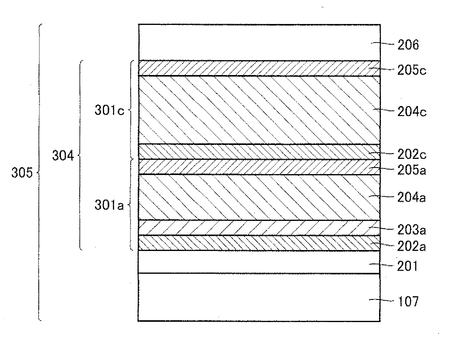
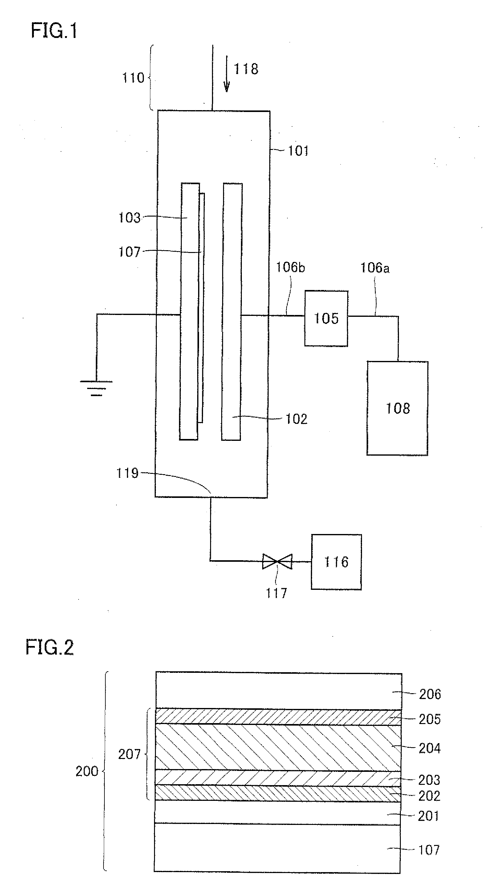
[0060]FIG. 2 is a schematic cross sectional view of a thin film photoelectric conversion element as a semiconductor device formed in Embodiment 1 of the present invention. A thin film photoelectric conversion element 200 shown in FIG. 2 has a structure including substrate 107, a first electrode 201, a semiconductor layer 207 having a first conductive layer 202, a buffer layer 203, a photoelectric conversion layer 204, and a second conductive layer 205, and a second electrode 206. In FIG. 2, the first conductive layer 202, buffer layer 203, photoelectric conversion layer 204, and the second conduc...

embodiment 2

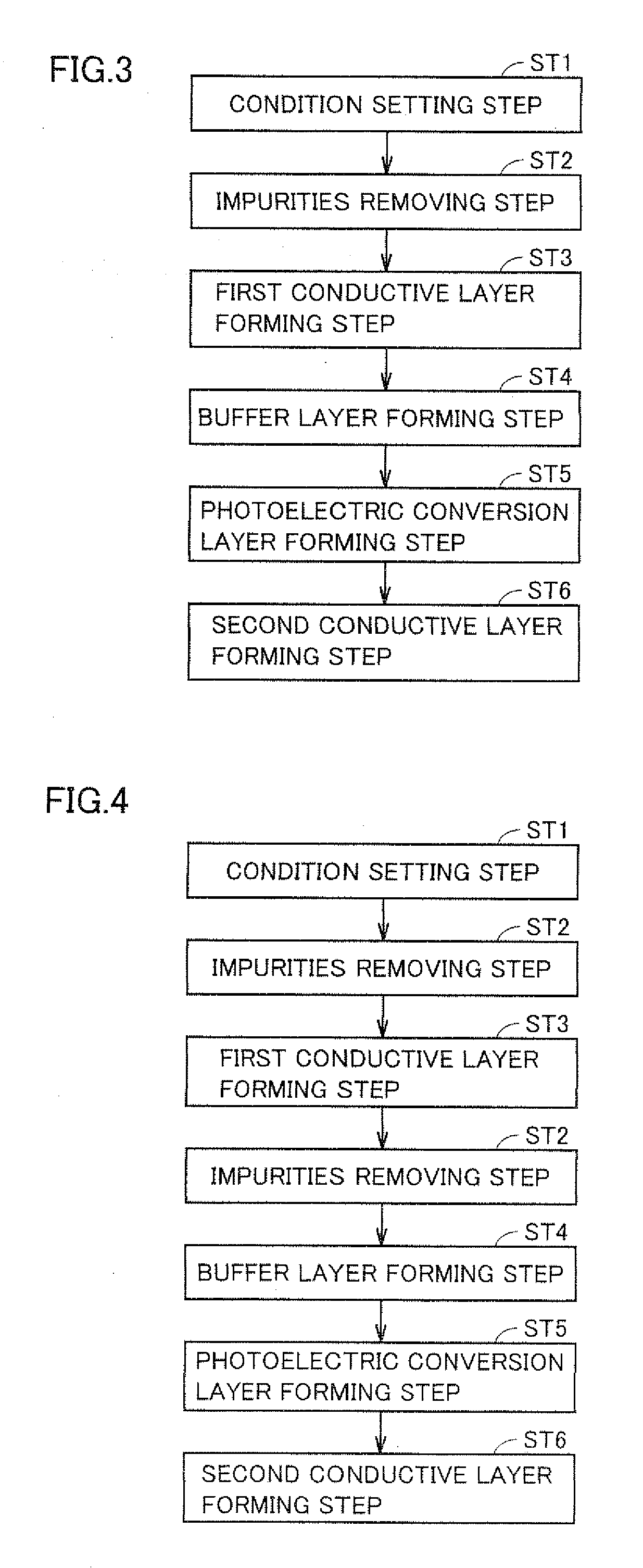
[0111]FIG. 4 is a flowchart of a semiconductor layer manufacturing method in accordance with Embodiment 2 of the present invention. In the present embodiment, a description will be given on a case where a semiconductor layer of a thin film photoelectric conversion element with a configuration shown in FIG. 2 is manufactured. In the present invention, it is preferable to further include the impurities removing step between the first conductive layer forming step and the buffer layer forming step. In the present embodiment, a description will be given on a case where tile impurities removing step (ST2) is further performed after the first conductive layer forming step (ST3) and before the buffer layer forming step (ST4). Since other steps can be performed as in Embodiment 1, the description thereof will not be repeated.

[0112]In the impurities removing step (ST2) performed after the first conductive layer forming step (ST3), the gas replacement operation can be repeatedly performed fou...

embodiment 3

[0116]FIG. 5 is a flowchart of a semiconductor layer manufacturing method in accordance with Embodiment 3 of the present invention. In the present embodiment, a description will be given on a case where a semiconductor layer of a thin film photoelectric conversion element with a configuration shown in FIG. 2 is manufactured. In the present invention, it is preferable to further include the impurities removing step between the buffer layer forming step and the photoelectric conversion layer forming step. In the present embodiment, a description will be given on a case where the impurities removing step (ST2) is further performed after the buffer layer forming step (ST4) and before the photoelectric conversion layer forming step (ST5). Since other steps can be performed as in Embodiment 1, the description thereof will not be repeated. The number of repeating the gas replacement operation in the impurities removing step is determined as in Embodiment 2, and is set to four times.

[0117]B...


PUM

PropertyMeasurementUnit
Pressureaaaaaaaaaa
Pressureaaaaaaaaaa
Pressureaaaaaaaaaa

Abstract

Provided are a semiconductor layer manufacturing method and a semiconductor manufacturing apparatus capable of forming a high quality semiconductor layer even by a single chamber system, with a shortened process time required for reducing a concentration of impurities that exist in a reaction chamber before forming the semiconductor layer. A semiconductor device manufactured using such a method and apparatus is also provided. The present invention relates to a semiconductor layer manufacturing method of forming a semiconductor layer inside a reaction chamber (101) capable of being hermetically sealed, including an impurities removing step of removing impurities inside the reaction chamber (101) using a replacement gas, and a semiconductor layer forming step of forming the semiconductor layer, the impurities removing step being a step in which a cycle composed of a replacement gas introducing step of introducing the replacement gas into the reaction chamber (101) and an exhausting step of exhausting the replacement gas is repeated a plurality of times, the impurities removing step being performed at least before the semiconductor layer forming step.

Description

TECHNICAL FIELD[0001]The present invention relates to a semiconductor layer manufacturing method, a semiconductor layer manufacturing apparatus, and a semiconductor device manufactured using such a method and apparatus. More specifically, the present invention relates to a semiconductor layer manufacturing method and a semiconductor layer manufacturing apparatus for manufacturing a semiconductor layer made of semiconductor thin films by a single chamber system, using for example plasma CVD or the like, and a semiconductor device manufactured using such a method and apparatus.BACKGROUND ART[0002]Recently, thin film photoelectric conversion elements formed by plasma CVD using a gas as a raw material have been attracting attention. Examples of such thin film photoelectric conversion elements include a silicon-based thin film photoelectric conversion element made of silicon-based thin films, a thin film photoelectric conversion element made of a CIS (CuInSe2) compound or a CIGS (Cu(In, ...

Claims


Application Information

Patent Timeline
IPC IPC(8): H01L31/075H01L21/20H01L31/0352B05C11/115H01L21/205H01L31/076H01L31/077H01L31/18
CPCC23C16/4408Y02E10/547H01L21/02532H01L21/02573H01L21/02592H01L21/02595H01L21/0262H01L21/02661H01L31/0747H01L31/075H01L31/1804H01L31/1816H01L31/202Y02E10/548C23C16/45557Y02P70/50
Inventor KISHIMOTO, KATSUSHIFUKUOKA, YUSUKE
Owner SHARP KK
Why Eureka
Try Eureka