
Photon trapping solar cell

a solar cell and photon technology, applied in the field of photon trapping solar cells, can solve the problems of increasing raw material demands, limiting the supply of sun energy, and straining the demands of raw cds/cdte materials, and achieve the effect of reducing the efficiency barrier of cds/cdte cells and reducing the thickness of css/cdte cell designs

Inactive Publication Date: 2010-02-04
MCCLARY RICHARD L +1
View PDF5 Cites 6 Cited by
  • Summary
  • Abstract
  • Description
  • Claims
  • Application Information

AI Technical Summary

Benefits of technology

[0005]The present invention provides a solution to the efficiency barrier of CdS / CdTe cells by radically changing the design process for obtaining solutions for material thicknesses in the photovoltaic region and in the capturing of energy resulting in much thinner CsS / CdTe cell designs.
[0006]The design approach for efficient solar energy designs was invented using first Principles of Quantum Mechanics coupled with Particle-Wave Duality. This unique process led to extremely thin CdTe / CdS Cell thicknesses whereby freed electrons traverse through the cell media with only a minimum chance of recombining with the CdTe molecules thus resulting in preservation of energy. In addition, the design is optimized for trapping reflected electrons to add the energy on multiple passes through the region thus further enhancing the energy conversion.
[0008]The implications of this Invention to the US and the world energy policies is extremely broad and PTSC would open a new era of energy production. The supply of energy from the sun is almost limitless and if PTSC can harness this energy at affordable costs, the world can generate almost limitless energy in electricity. The energies of the oceans can be harnessed. Ocean waters can be converted to hydrogen gases for supplying heat and fuel cell engines, water can be obtained for deserts and farming at low costs. Miles and miles of open desert areas can be turned into energy farms supplying giga watts of energy to the power grid.
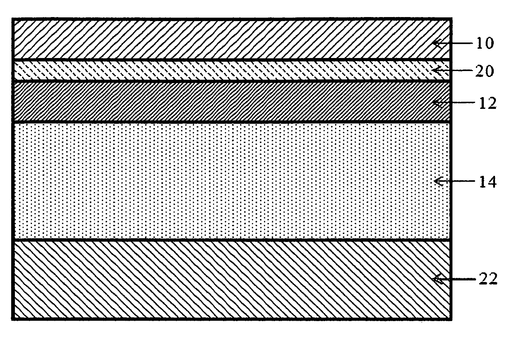
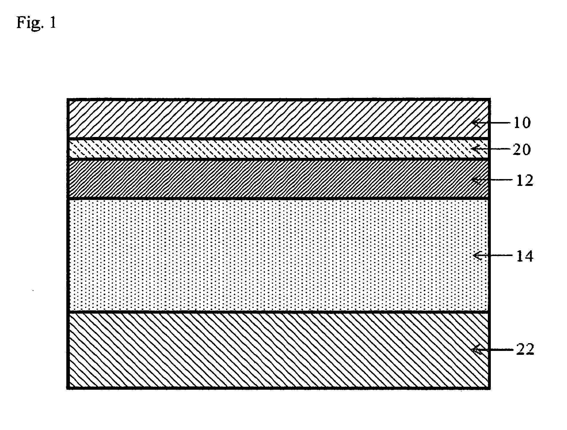
[0009]The Nano Structure CdTe PTSC solar cell unique multi layer construction allows the formation of a photon trapping geometry which results in high energy conversions. A preferred embodiment of the present invention comprises a 2 stack design between 96.75 nm and 387 nm thick with the following parameters: the upper layer comprises n-type photoelectric material, preferably CdS, and the bottom layer comprises p-type photoelectric material, preferably CdTe. Further, electrodes are attached to the top and bottom of the 2 layer stack, wherein the bottom electrode is a metallic reflective conductive material, for example aluminum. The PTSC may further comprise an antireflective 1 over the top electrode that also functions to protect the structure underneath

Problems solved by technology

Although Cadmium is readily available, the implication of large CdS / CdTe solar cell systems when implemented worldwide would increase raw material demands unless only a small amount of raw Cadmium Sulfide and Cadmium Telluride material is used in the designs.
Thin film solar cell designs are an answer but they would strain the demands of the raw CdS / CdTe material.
The supply of energy from the sun is almost limitless and if PTSC can harness this energy at affordable costs, the world can generate almost limitless energy in electricity.

Method used


Image

  • Photon trapping solar cell
  • Photon trapping solar cell
  • Photon trapping solar cell

Examples


example

[0038]Shown below is some of the output of a typical optimization run using programs optical_stack.f and optical_stack_opt.f. This run optimizes a two layer antireflection coating along with the layers of CdS and CdTe. These programs are written to assume that all thicknesses are in thickness units of Angstroms. Since most optical thicknesses are currently expressed in nanometers (1 nanometer=10 Angstroms), the final design thicknesses are converted from Angstroms to nanometers.

#AMOEBA SUMMARY FILE GENERATED Sat Mar 1 11:10:44 2008#NUMBER OF ANGLES = 10#Layer 1 Thick. Layer 2 Layer 3 Layer 4 loss Layer 4 Figure of merit# 760.000 450.000 300.000 0.500 3000.000 −3.936# 988.000 450.000 300.000 0.500 3000.000 −4.426# 760.000 585.000 300.000 0.500 3000.000 −3.621# 760.000 450.000 390.000 0.500 3000.000 −3.598# 760.000 450.000 300.000 0.650 3000.000 −5.055# 760.000 450.000 300.000 0.500 3900.000 −3.557#END OF INITIALIZATION # 1# 851.200 504.000 336.000 0.560 2100.000 −2.292# 782.800 463.5...


PUM


Abstract

A nano structure CdTe / CdS Photon Trapping Solar Cell (PTSC) comprising an ultra thin film stack construction of 2 layers, one each of Cadmium Sulfide and Cadmium Telluride, and wherein the bottom electrode is a reflecting sheet or plate that serves to reflect Photons unabsorbed by their pass through the material back through the layers of Cadmium Telluride and Cadmium Sulfide. The bottom metallic plate also serves as an electron conductor for allowing the photoelectric current to exit the device and perform useful work. The cell has a maximum efficiency of 40%.

Description

CROSS REFERENCE TO RELATED APPLICATIONS[0001]This application claims the benefit of U.S. Provisional Application No. 61 / 137,822 filed Aug. 4, 2008, the contents of which are incorporated herein by reference.BACKGROUND OF THE INVENTION[0002]Solar cell technology and design is rapidly converging to thin film CdTe techniques to reduce the high production cost of Silicon based solar cell technology. Thin film p-type CdTe with n-type CdS solar cells and systems have emerged as the one possible solution to replace Silicon solar cells. However, the conversion efficiency of thin film CdTe / CdS solar cells presently available are far short of Silicon Cells and have not reached a point where government subsidies are not required for effective commercialization to compete with conventional energy production. Typical proven efficiencies of only 9 percent are presently reported by large commercial companies. Today's CdTe / CdS solar cell systems designs cannot compete directly with the economic cos...

Claims


Application Information

Patent Timeline
Patent Type & Authority Applications(United States)
IPC IPC(8): H01L31/00H01L31/18
CPCH01L31/0296H01L31/056Y02E10/52H01L31/035272
Inventor MCCLARY, RICHARD L.TOMITA, CHARLES Y.
Owner MCCLARY RICHARD L
Learn More