Wide band gap semiconductor device including junction field effect transistor

a semiconductor device and junction field effect technology, applied in the direction of semiconductor devices, basic electric elements, electrical appliances, etc., can solve the problems of difficult to improve the breakdown voltage of the semiconductor device, the oxide layer may easily break down, etc., to achieve high breakdown voltage

Active Publication Date: 2010-02-04
DENSO CORP +1
View PDF3 Cites 60 Cited by
  • Summary
  • Abstract
  • Description
  • Claims
  • Application Information

AI Technical Summary

Problems solved by technology

When a semiconductor device has an isolation structure including a trench filled with an oxide layer, a breakdown may occur at an end portion of a schottky diode, and the oxide layer may breakdown.
Thus, the oxide layer may breakdown easily.
Thus, even if a breakdown voltage of the JFET and a breakdown voltage of the schottky diode are increased, the breakdown voltage of the semiconductor device is difficult to be improved.
Therefore, the electric current locally flows and a breakdown voltage of the semiconductor device is difficult to be improved.
However, the above-described issue may also occur in a semiconductor device including another wide gap semiconductor such as gallium nitride (GaN) and diamond.

Method used


Image

  • Wide band gap semiconductor device including junction field effect transistor
  • Wide band gap semiconductor device including junction field effect transistor
  • Wide band gap semiconductor device including junction field effect transistor

Examples


first embodiment

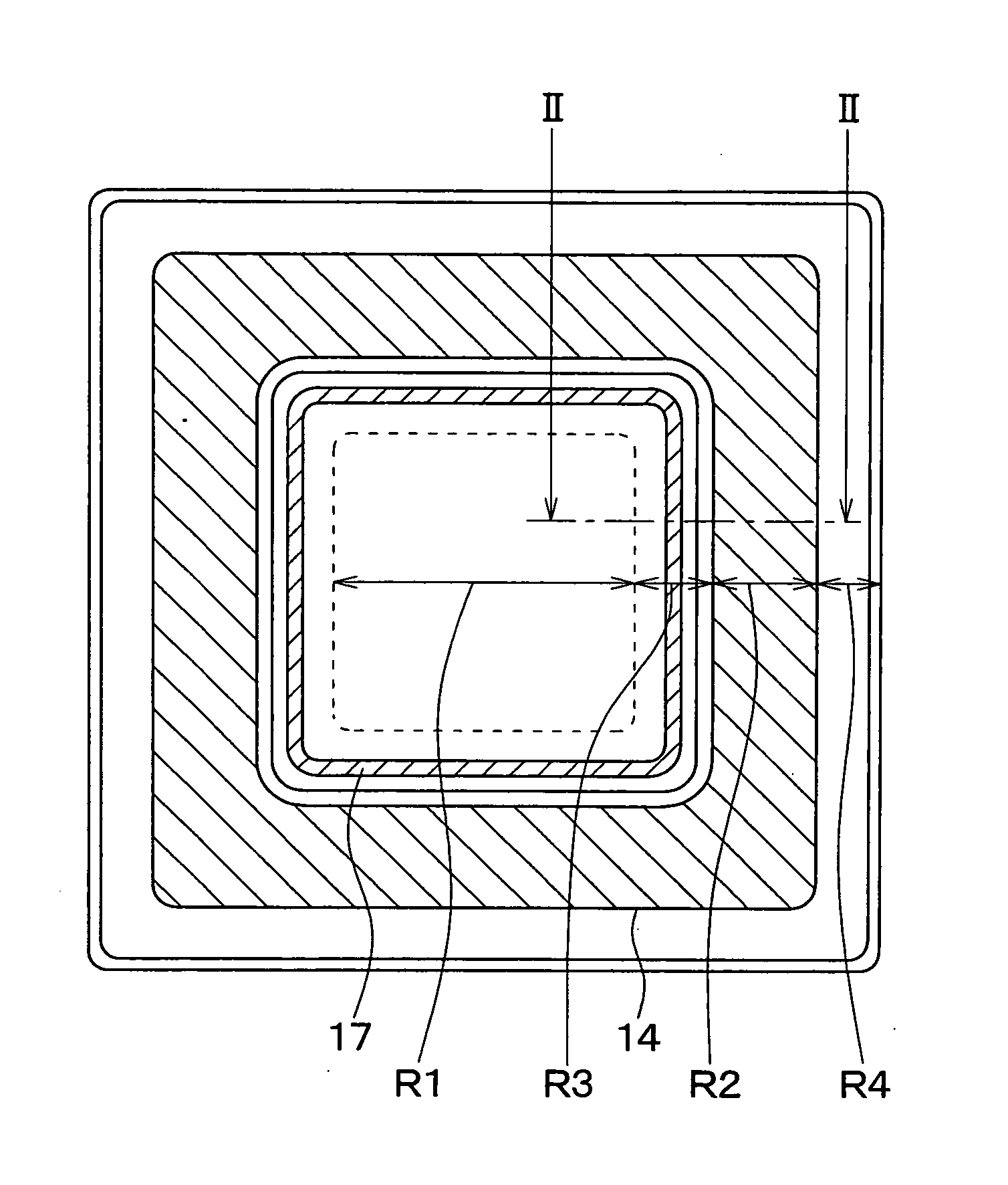
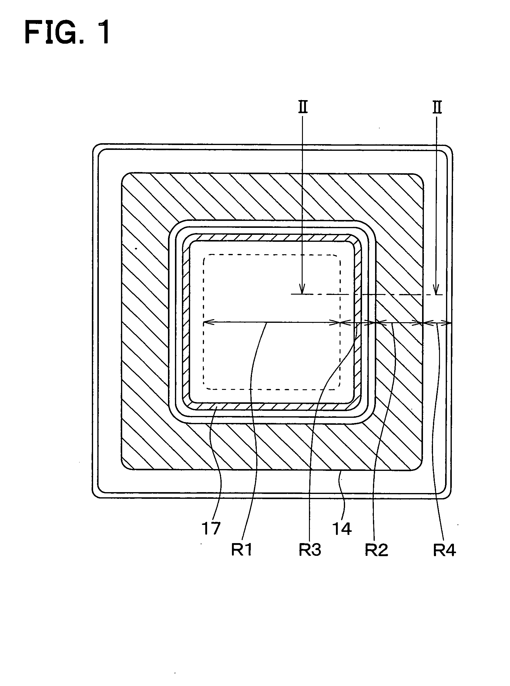
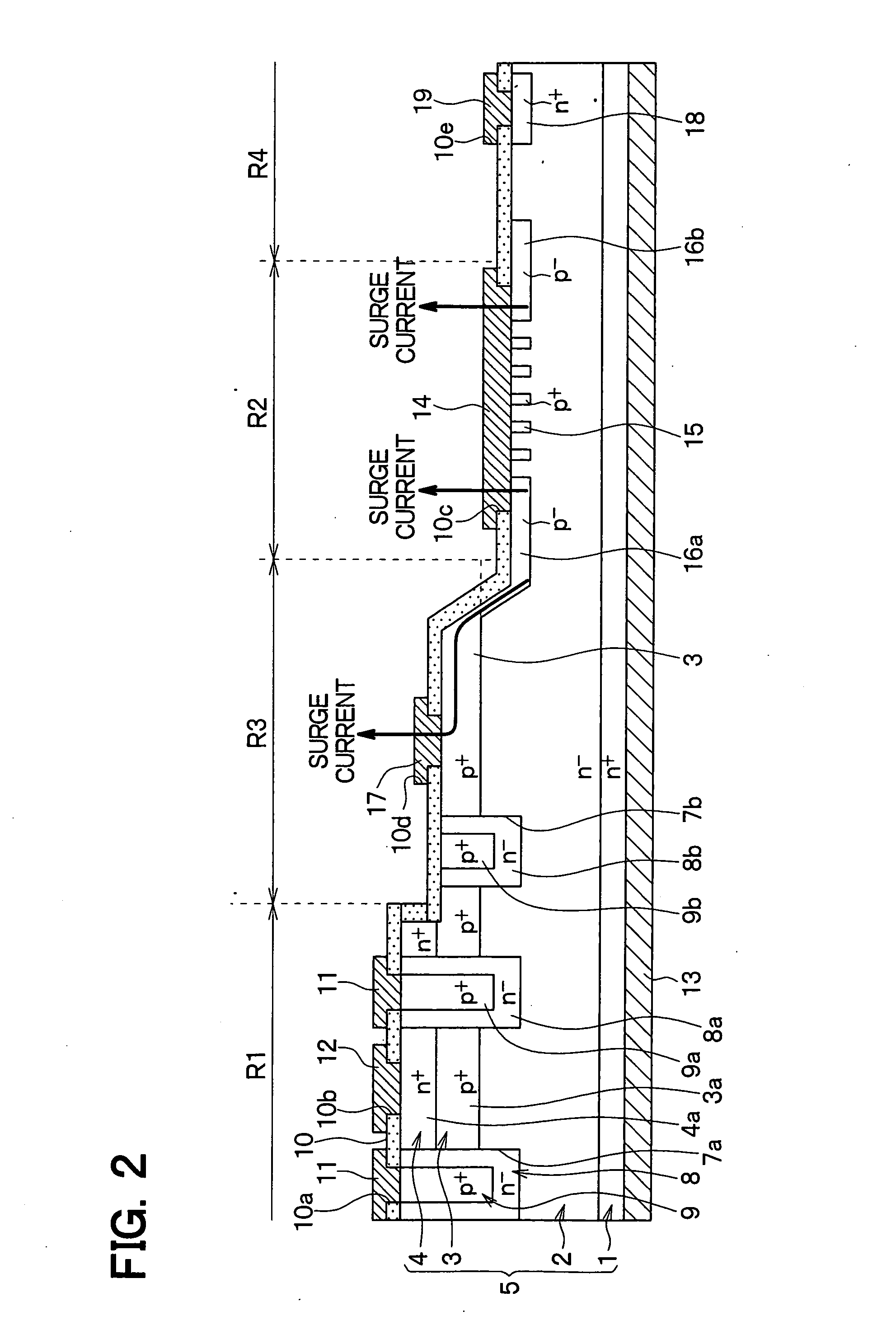
[0036]An SiC semiconductor device according to a first embodiment of the present invention will be described with reference to FIG. 1 and FIG. 2.

[0037]The SiC semiconductor device includes a transistor cell region R1, a diode forming region R2, an electric field relaxation region R3, and an outer peripheral region R4. At the transistor cell region R1, a plurality of JFETs is formed. The transistor cell region R1 has an approximately square shape with rounded corners in top view. At the diode forming region R2, a JBS is formed as a diode. The diode forming region R2 has an approximately square frame shape with rounded corners in top view and surrounds the transistor cell region R1. The electric field relaxation region R3 is located between the transistor cell region R1 and the diode forming region R2. The electric field relaxation region R3 has an approximately square frame shape with rounded corners in top view and surrounds the transistor cell region R1. The electric field relaxati...

second embodiment

[0079]An SiC semiconductor device according to a second embodiment of the present invention will be described with reference to FIG. 14 and FIG. 15.

[0080]The SiC semiconductor device includes a transistor cell region R1, a diode forming region R2, an electric filed relaxation region R3 and an outer peripheral region R4. Diode forming region R2 is located at a center portion of the semiconductor substrate 5. The transistor cell region R1 surrounds the diode forming region R2. The electric field relaxation region R3 is disposed between the transistor cell region R1 and the diode forming region R2 so as to surround the diode forming region R2. The outer peripheral region R4 surrounds the transistor cell region R1. The electric field relaxation region R3 is further located between the transistor cell region R1 and the outer peripheral region R4 so as to surround the transistor cell region R1. As illustrated in FIG. 15, each of the transistor cell region R1, the diode forming region R2, ...

third embodiment

[0082]An SiC semiconductor device according to a third embodiment of the present invention, will be described with reference to FIG. 16. In the SiC semiconductor device according to the present embodiment, each of a diode forming region R2 and an outer peripheral region R4 has a configuration different from a corresponding region in the SiC semiconductor device according to the first embodiment. Other regions in the SiC semiconductor device according to the present embodiment are similar to corresponding regions in the SiC semiconductor device according to the first embodiment. Thus, a part different from the first embodiment will be mainly described.

[0083]A portion in the vicinity of the diode forming region R2 in the SiC semiconductor device according to the present embodiment is illustrated in FIG. 16. As illustrated in FIG. 16, the diode forming region R2 includes a PN diode. For example, the P+ type layer 3 and the N+ type drift layer 2 formed in the semiconductor substrate 5 c...


PUM


Abstract

A wide band gap semiconductor device has a transistor cell region, a diode forming region, an electric field relaxation region located between the transistor cell region and the diode forming region, and an outer peripheral region surrounding the transistor cell region and the diode forming region. In the transistor cell region, a junction field effect transistor is disposed. In the diode forming region, a diode is disposed. In the electric field relaxation region, an isolating part is provided. The isolating part includes a trench dividing the transistor cell region and the diode forming region, a first conductivity-type layer disposed on an inner wall of the trench, and a second conductivity-type layer disposed on a surface of the first conductivity-type layer so as to fill the trench. The first conductivity-type layer and the second conductivity-type layer provide a PN junction.

Description

CROSS REFERENCE TO RELATED APPLICATIONS[0001]The present application is based on and claims priority to Japanese Patent Application No. 2008-196107 filed on Jul. 30, 2008, the contents of which are incorporated in their entirety herein by reference.BACKGROUND OF THE INVENTION[0002]1. Field of the Invention[0003]The present invention relates to a wide band gap semiconductor device including a junction filed effect transistor (JFET).[0004]2. Description of the Related Art[0005]US 2006 / 0011924 A discloses a semiconductor device including a transistor cell region in which a JFET is disposed and an outer peripheral region in which a schottky diode and an outer peripheral withstand-voltage part are disposed. In the above-described semiconductor device, a trench is provided between the transistor cell region and the outer peripheral region and the trench is filled with an oxide layer, and thereby the transistor cell region and the outer peripheral region are isolated from each other.[0006]...

Claims


Application Information

Patent Timeline
Patent Type & Authority Applications(United States)
IPC IPC(8): H01L29/772H01L29/02
CPCH01L29/063H01L29/0692H01L29/6609H01L29/872H01L29/8083H01L29/8611H01L29/66325
Inventor MALHAN, RAJESH KUMARTAKEUCHI, YUUICHIRASHID, JEREMY
Owner DENSO CORP
Why Eureka
Try Eureka