Semiconductor device and method of manufacturing the same

a technology of semiconductor devices and semiconductors, applied in the direction of semiconductor devices, basic electric elements, electrical appliances, etc., can solve the problems of inability to properly draw both performances, and achieve the effect of optimizing the characteristics of vertical switching devices, improving carrier mobility characteristics, and narrowing the pitch of transistors

Inactive Publication Date: 2010-02-11
SONY CORP
View PDF1 Cites 20 Cited by
  • Summary
  • Abstract
  • Description
  • Claims
  • Application Information

AI Technical Summary

Benefits of technology

[0030]When the arrangement pitch of the control electrodes of the vertical switching device is not restricted by the arrangement pitch of the pn pillar pairs having the super-junction structure, the vertical switching device can be manufactured in accordance with a miniaturization optimal rule for the process. Also, the arrangement pitch of the pn pillar pairs can be optimized from the aspect of the ON resistance and the withstand voltage. The crystal plain orientation allowing the carrier mobility characteristics to be improved is made to appear in each of the sidewalls of the trenches for the control electrodes, thereby making it possible to optimize the characteristics of the vertical switching device.

Problems solved by technology

Thus, it may be impossible to pro

Method used


Image

  • Semiconductor device and method of manufacturing the same
  • Semiconductor device and method of manufacturing the same
  • Semiconductor device and method of manufacturing the same

Examples


first embodiment

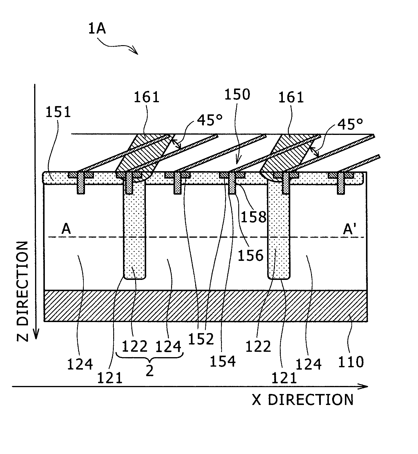
[0060]FIGS. 3A and 3B are respectively views each showing a structure of a semiconductor device 1A according to a first embodiment of the present invention. Here, FIG. 3A is a top plan view schematically showing the structure of the semiconductor device 1A, and FIG. 1B is a bird's eye view obtained by paying attention to an XZ cross sectional view taken on line A-A′ of FIG. 3A. FIGS. 3A and 3B are each schematic views, and thus the present invention is by no means limited to the sizes in these figures. This also applies to any of other embodiments which will be described later.

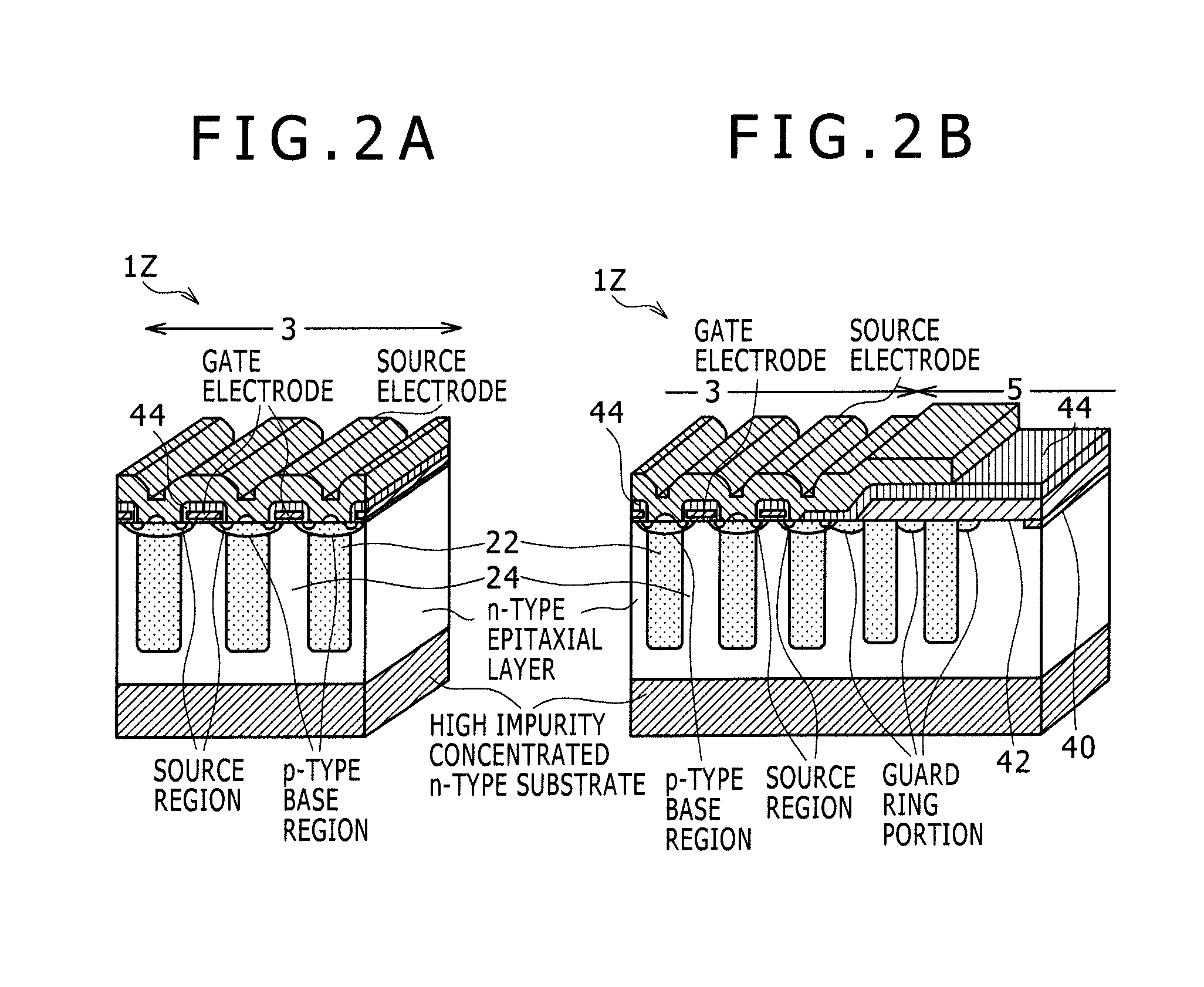
[0061]The semiconductor device 1A of the first embodiment includes an n-type epitaxial layer 120 (a second semiconductor region of a first conductivity type) on a surface of a high impurity concentrated n-type substrate 110 (an n+-type drain layer) as an example of a first semiconductor region of the first conductivity type having a relatively high impurity concentration. Here, the n-type epitaxial layer 120 i...

second embodiment

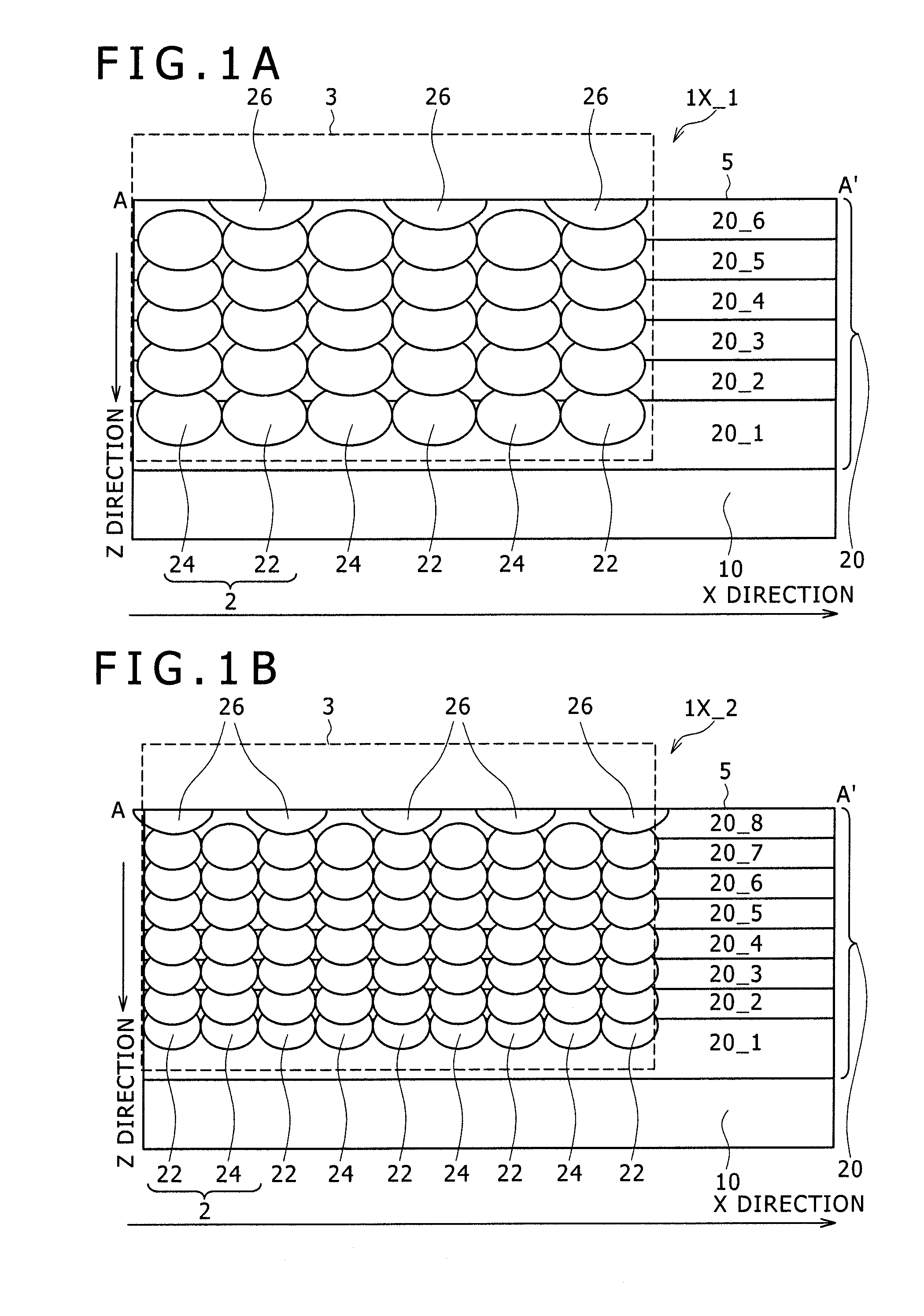
[0090]FIGS. 4A and 4B are respectively views showing a structure of a semiconductor device 1B according to a second embodiment of the present invention. Here, FIG. 4A is a top plan view schematically showing the structure of the semiconductor device 1B, and FIG. 4B is a bird's eye view obtained by paying attention to an XZ cross section taken on line A-A′ of FIG. 4A.

[0091]In the semiconductor device 1B of the second embodiment, the disposition form of the vertical MOSFET 150 is slightly changed while the structure of the first embodiment is basically applied to the super-junction structure. The feature of the basic way of thinking about the change is that although in the vertical MOSFET, the gate oxide film 156 and the gate electrode 158 of the gate are formed within the shallow trench 154, the gate electrodes 158 extend in parallel at an angle of 45° with each other on both sides of the Y-axis direction in the figures (that is, at the angles of ±45° with the Y-axis direction). That...


PUM


Abstract

Disclosed herein is a semiconductor device, including: a first semiconductor region of a first conductivity type; a second semiconductor region having pairs of first pillar regions of the first conductivity type, and second pillar regions of a second conductivity type alternately provided; a third semiconductor region of the second conductivity type; a fourth semiconductor region of the first conductivity type; and control electrodes each provided within a trench through an insulating film, a sidewall of the trench being formed so as to contact each of the third semiconductor region and the fourth semiconductor region.

Description

BACKGROUND OF THE INVENTION[0001]1. Field of the Invention[0002]The present invention relates to a semiconductor device and a method of manufacturing the same, and more particularly to a semiconductor device having a super-junction structure, and a method of manufacturing the same.[0003]2. Description of the Related Art[0004]In recent years, a request for thinning and weight saving for electronic apparatuses has been strong as represented by a liquid crystal television set, a plasma television set, an organic EL (Electro-Luminescence) television set, and the like. Along with the above request, a request for miniaturization and promotion of high performance for power source apparatuses has also been strong. In response to this request, in a power semiconductor element, performance improvements such as high withstand voltage promotion, large current promotion, low loss promotion, high speed promotion and high breaking withstand voltage promotion have attracted attention. For example, ...

Claims


Application Information

Patent Timeline
IPC IPC(8): H01L29/78H01L21/28H01L21/336
CPCH01L29/045H01L29/0619H01L29/0634H01L29/0638H01L29/7813H01L29/1095H01L29/4238H01L29/66734H01L29/7811H01L29/0696H01L21/02225
Inventor HOZUMI, HIROKISASAKI, YUJIYANAGAWA, SHUSAKU
Owner SONY CORP
Why Eureka
Try Eureka