Method of Manufacture of a Multi-Layer Phosphorescent Organic Light Emitting Device, and Articles Thereof

a phosphorescent organic light emitting device and multi-layer technology, applied in the direction of discharge tube luminescnet screen, other domestic articles, organic semiconductor devices, etc., can solve the problems of low manufacturing throughput, high cost and low manufacturing throughput, and the fabricated multi-emission phosphorescent oleds via solvent coating

Inactive Publication Date: 2010-02-11
GENERAL ELECTRIC CO
View PDF22 Cites 23 Cited by
  • Summary
  • Abstract
  • Description
  • Claims
  • Application Information

AI Technical Summary

Problems solved by technology

Multi-layered phosphorescent OLEDs based on small molecules are typically produced via vacuum deposition of the organic materials, which is disadvantaged by high cost and low manufacturing throughput.
Multi-emission phosphorescent OLEDs fabricated via solvent coating such as gravure coating, screen-printing, and other solvent coating methods have not been demonstrated, although ...

Method used


Image

  • Method of Manufacture of a Multi-Layer Phosphorescent Organic Light Emitting Device, and Articles Thereof
  • Method of Manufacture of a Multi-Layer Phosphorescent Organic Light Emitting Device, and Articles Thereof
  • Method of Manufacture of a Multi-Layer Phosphorescent Organic Light Emitting Device, and Articles Thereof

Examples


example

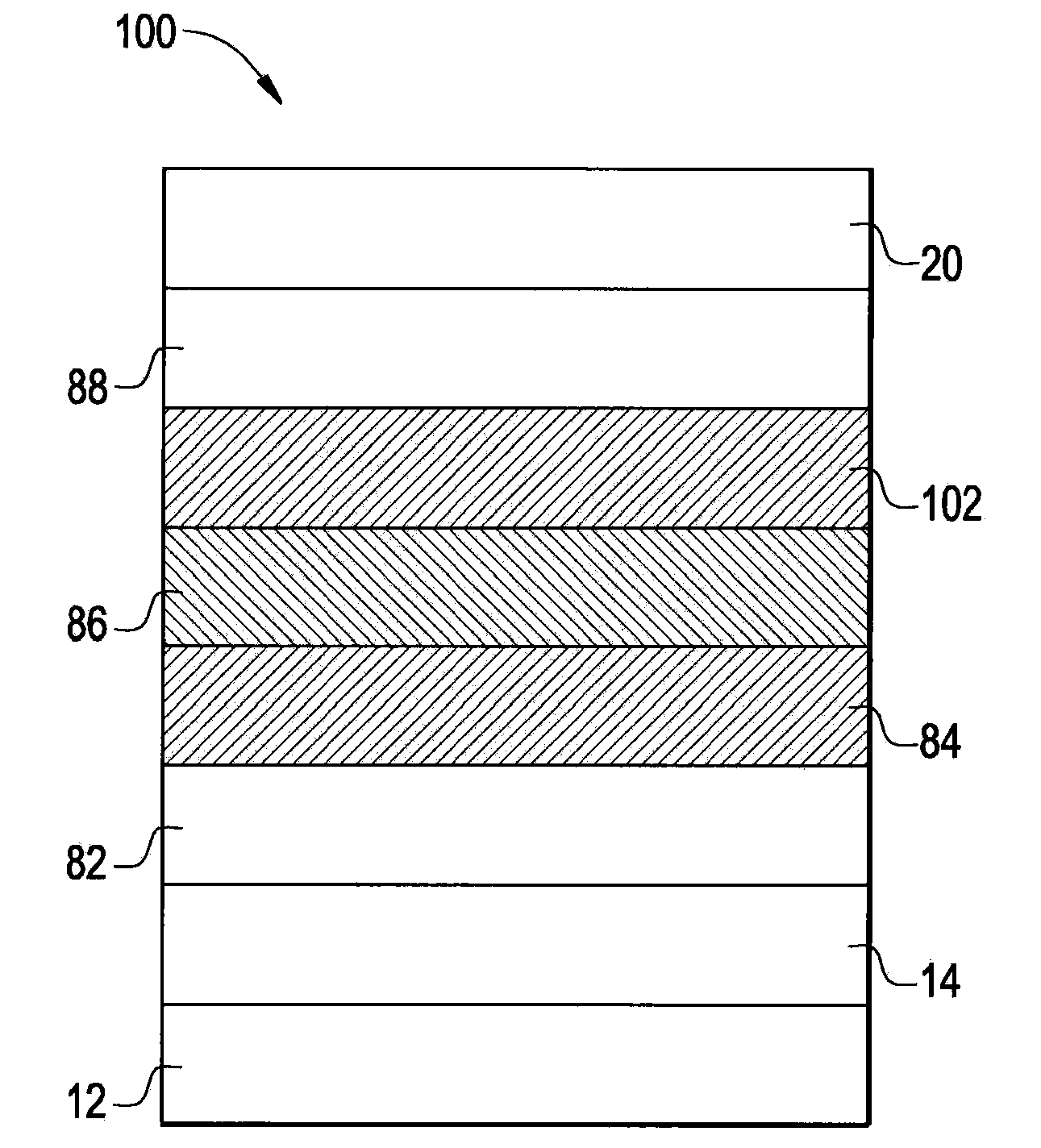
[0082]A multi-layered phosphorescent OLED was constructed as follows. The phosphorescent OLED comprises a blue phosphorescent polymer emissive layer and a red phosphorescent emissive layer. Pre-patterned ITO coated glass was used as the anode substrate, and was cleaned with UV-ozone for 10 minutes. A layer (60 nm) of poly(3,4-ethylendioxythiophene) doped with polystyrene sulfonic acid (PEDOT:PSS) obtained from H.C. Starck was deposited atop the ITO via spin-coating and then baked for 1 hour at 180° C. in air. The coated substrate was then transferred into a glovebox filled with argon (both moisture and oxygen were less than 1 ppm). The blue phosphorescent polymer emissive layer of 275-44-5 (approximately 30 nm thickness) was then spin-coated from solution in chlorobenzene atop the PEDOT:PSS layer and baked on a hotplate (pre-heated to 120° C.) for 10 minutes. Next, a mixture of OXD-7 (1,3-bis[(p-tert-butyl)phenyl-1,3,4-oxadiazoyl]benzene), purchased from H.W. Sands and used as recei...


PUM

PropertyMeasurementUnit
Solubility (mass)aaaaaaaaaa
Emissivityaaaaaaaaaa
Phosphorescence quantum yieldaaaaaaaaaa

Abstract

A method for forming multi-emissive phosphorescent layers for a phosphorescent OLED comprises coating a first phosphorescent material from a first solvent onto a first electrode and removing the first solvent to form a first emissive layer; and coating a second phosphorescent material from a second solvent onto the first emissive layer and removing the second solvent to form a second emissive layer, wherein the first and second emissive layers are not cured after coating, and wherein the first emissive layer has negligible solubility in the second solvent.

Description

BACKGROUND OF THE INVENTION[0001]This disclosure relates generally to a method of manufacture of multi-layer, phosphorescent organic light emitting devices, and articles thereof.[0002]Organic light emitting devices (OLEDs) with multi-layered structures are generally preferred to achieve high performance and meet specific requirements such as white light required for illumination. Phosphorescent emissive materials in OLEDs are desirable because they can potentially achieve 100% internal quantum efficiency (IQE) relative to 25% IQE for fluorescent emissive materials.[0003]Current state-of-the-art phosphorescent emissive materials are available as small molecules. Multi-layered phosphorescent OLEDs based on small molecules are typically produced via vacuum deposition of the organic materials, which is disadvantaged by high cost and low manufacturing throughput.[0004]Multi-emission phosphorescent OLEDs fabricated via solvent coating such as gravure coating, screen-printing, and other so...

Claims


Application Information

Patent Timeline
IPC IPC(8): H01L51/52H01J1/63B05D5/12
CPCC08G2261/1424C08G2261/3223C08G2261/512H01L51/0007H01L51/0037H01L2251/5361H01L51/0043H01L51/0072H01L51/0085H01L51/5016H01L51/5036H01L51/004H10K71/15H10K85/1135H10K85/141H10K85/151H10K85/342H10K85/6572H10K50/125H10K50/11H10K2101/10Y10S428/917
Inventor LIU, JIECHICHAK, KELLY SCOTTDUGGAL, ANIL RAJYE, QING
Owner GENERAL ELECTRIC CO
Why Eureka
Try Eureka