Clock adjusting circuit and semiconductor integrated circuit device

a clock-adjusting circuit and integrated circuit technology, applied in the direction of generating/distributing signals, pulse techniques, instruments, etc., can solve the problems of not being able to detect faults or failures, operational faults on actual products, and not being able to test the margin while adjusting the operation frequency of lsi, so as to reduce false negatives of faults, high reliability, and large margin

Inactive Publication Date: 2010-02-18
NEC CORP
View PDF9 Cites 85 Cited by
  • Summary
  • Abstract
  • Description
  • Claims
  • Application Information

AI Technical Summary

Benefits of technology

[0124]According to the present invention, a clock adjusting circuit for adjusting a period, a duty, skew, and the like of a clock signal is mounted in a semiconductor integrated circuit device; and in an LSI mounted in a circuit board of an actual device or a test circuit board simulating an actual device, by giving a disturbance to a parameter of the clock signal inside the LSI while operating the semiconductor integrated circuit device, and detecting an operation margin with regard to the disturbance, it is possible to select the LSI with high reliability and with a large margin. According to the present invention, it is possible to detect a fail or fault in the LSI under conditions more severe than in conventional LSI tests.
[0125]According to the present invention, it is possible to give a disturbance to a clock signal of a limitless or an arbitrary number of cycles that are consecutive. As a result, it is possible to further reduce false negatives of faults or fails, and an effect is obtained in which it is possible to select and ship a semiconductor integrated circuit device with higher reliability.
[0126]According to the present invention, since a phase obtained by dividing one clock period (360 degrees) by N is a change amount for one adjustment stage, is it easy to comprehend an absolute value of time and phase of the operation margin from a test result.
[0127]Furthermore, according to the present invention, it is possible to realize, for a clock, effects which are
[0128](1) phase of two edges can be dynamically controlled,
[0129](2) adjustment range of a clock phase changed in one cycle is large, and

Problems solved by technology

With the increasing scale of LSI and increasing complexity of functions, there is often a case wherein it is not possible to detect a fault or fail only by testing a critical path of logic delay.
An LSI that has passed the test causes an operational fault on an actual product on which the LSI is mounted.
However, as described above, when a test of an LSI is performed under the condition that the LSI is mounted on the printed circuit board, it is not possible to test the margin while adjusting operational frequency of the LSI.
With respect to this type of interface, since the operational frequency, allowable duty ratio, and the like, are not prescribed by a specification, it is not possible to change the frequency of a system reference clock, in order to perform an operation by the overall system.
The oscillation frequency of this crystal oscillator is determined at the time of manufacture, and it is not possible to perform adjustment thereafter.
Since a clock signal inside an LSI, in general, is generated by a Phase Locked Loop (referred to as PLL), it is not possible to adjust duty ratio or the like of the clock signal inside the LSI from outside the LSI.
Thus, with regard to an LSI mounted on a printed circuit board, it is not possible to adjust a clock signal from the outside.
As a result, adjusting duty ratio, phase offset, or the like, of a clock inside the semiconductor integrated circuit from outside is not possible as long as a dedicated circuit for adjusting these is not provided.
Conversely, when switching is performed so that the delay is increased, a next clock phase is delayed, and the clock period of this instant is elongated.
Though this system can with ease perform expansion and shortening of the clock period, the number of clock cycles in which the clock period can be expanded and shortened is limited by the number of stages of delay element.
Since the delay amount of one delay element stage fluctuates due to variations, a user cannot accurately know how much the clock period fluctuates, by one-stage switching of the delay.
If a phase shift is performed by this circuit, a phase of a clock signal becomes unstable at an instant at which a value of the control signal changes and the phase shifter switches a clock phase.
This results in generating jitter that is not intended by a user.
In case the control signal is operated with a period the same as a clock period, since only a phase of an edge on one side of the clock signal can be shifted, it is not possible to adjust duty.

Method used


Image

  • Clock adjusting circuit and semiconductor integrated circuit device
  • Clock adjusting circuit and semiconductor integrated circuit device
  • Clock adjusting circuit and semiconductor integrated circuit device

Examples


Embodiment Construction

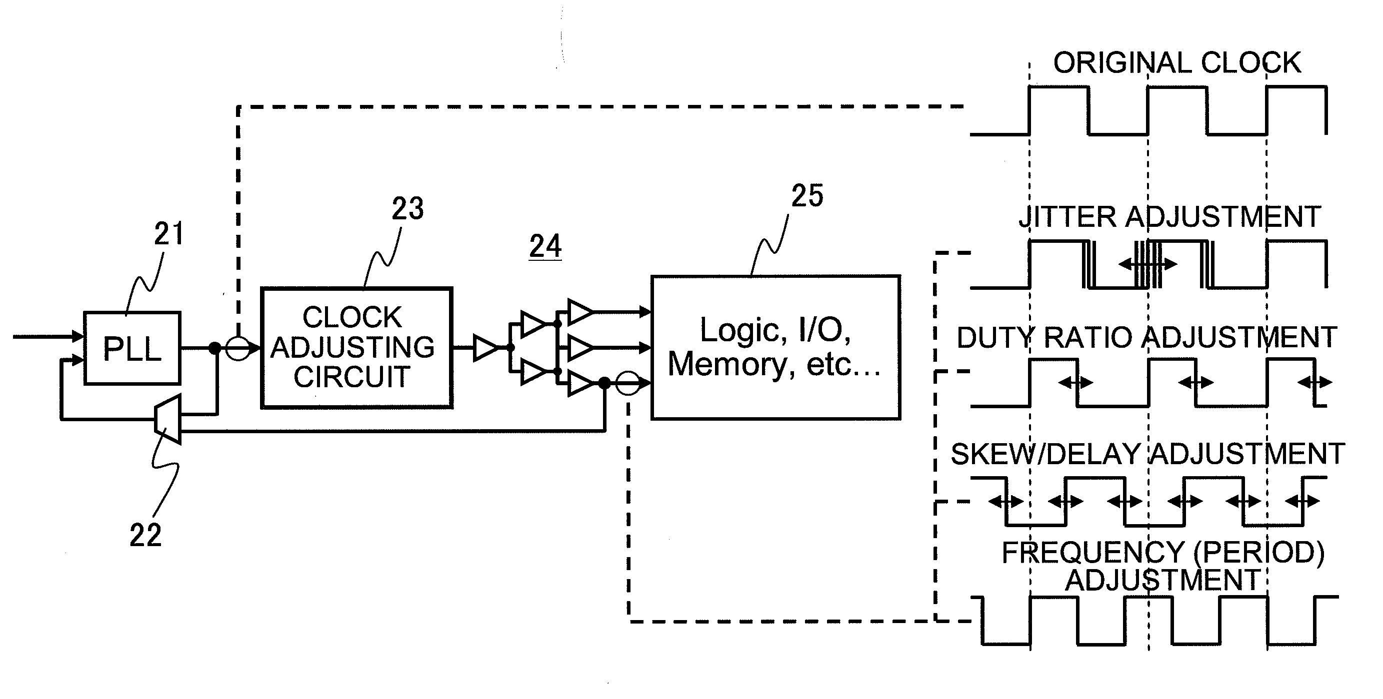
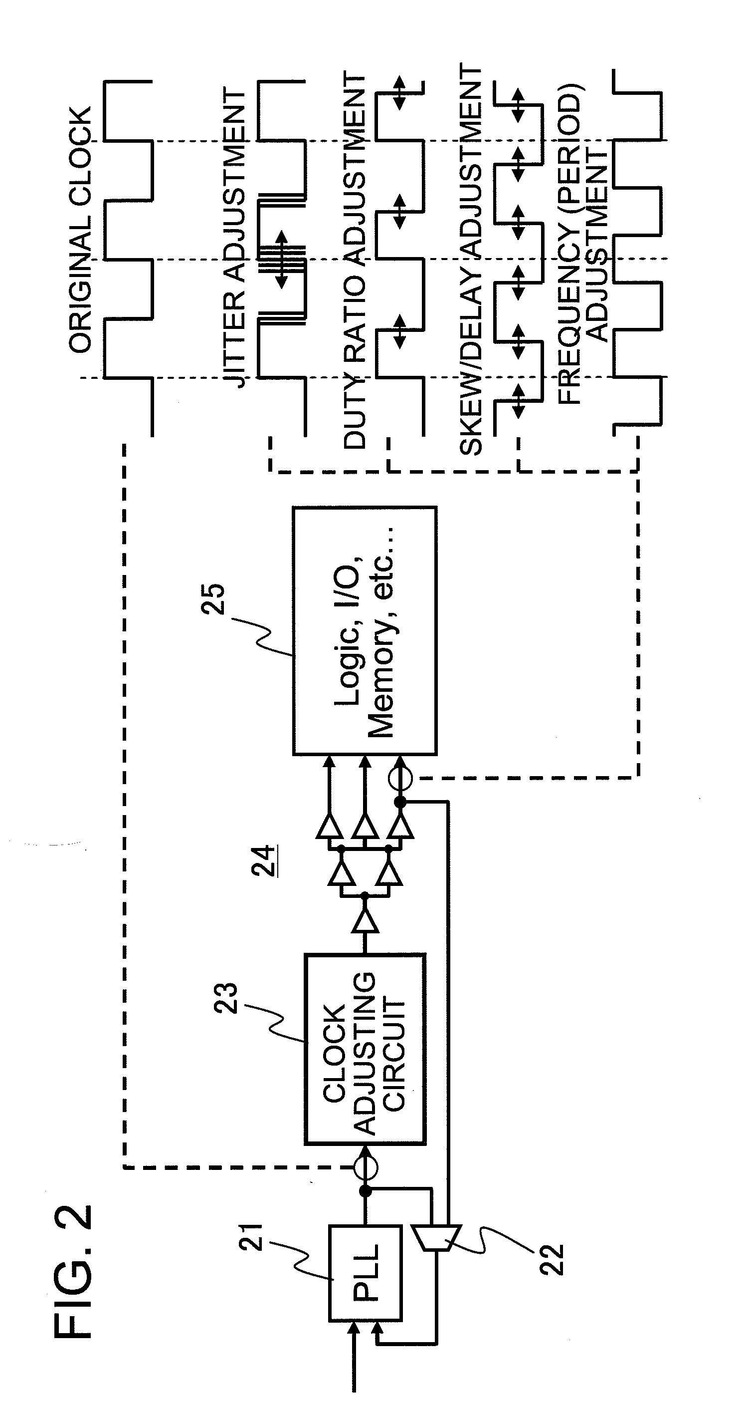
[0332]In the present invention, a semiconductor integrated circuit includes a circuit that can adjust a clock period, duty ratio, skew between clock domains, and the like, is built in a semiconductor integrated circuit. When the semiconductor integrated circuit is being tested, this circuit is used to perform an operation test while adjusting the clock period of a clock signal, duty, skew between the clock domains, and the like, inside a semiconductor integrated circuit, and to detect operation margin of each thereof. An LSI (Device Under Test) with little operation margin does not pass a selection test, and only semiconductor integrated circuits with a large margin are shipped.

[0333]Furthermore, using this adjustment circuit also after shipping of the semiconductor integrated circuit, a self test of the margin is performed with respect to the clock period, the duty, the skew, and the like, and in case the margin is less than a specified value, an operation of emitting a warning, or...


PUM


Abstract

Disclosed is a clock adjusting circuit comprising a phase shifter that receives a clock signal and variably shifts, based on a control signal, respective timing phases of a rising edge and a falling edge of the clock signal; and a control circuit that supplies the control signal to the phase shifter circuit before each edge is output; wherein the clock signal, in which at least one of a period, a duty ratio, jitter and skew/delay of the input clock signal is changed over an arbitrary number of clock cycles, is output.

Description

CROSS-REFERENCE TO RELATED APPLICATIONS[0001]This application is based upon and claims the benefit of the priority of Japanese patent applications No. 2006-247980 filed on Sep. 13, 2006 and No. 2007-021159 filed on Jan. 31, 2007, the disclosures of which are incorporated herein in their entirety by reference thereto.TECHNICAL FIELD[0002]The present invention relates to technology for improving reliability of semiconductor integrated circuits, and circuits for realization thereof; and, in particular, relates to operation margin test technology for the semiconductor integrated circuits and to clock signal generation technology for realizing the test.BACKGROUND ART[0003]Device screening test and operation margin test of conventional semiconductor integrated circuits are performed by an LSI tester. With the increasing scale of LSI and increasing complexity of functions, there is often a case wherein it is not possible to detect a fault or fail only by testing a critical path of logic de...

Claims


Application Information

Patent Timeline
Patent Type & Authority Applications(United States)
IPC IPC(8): H03K3/013
CPCG06F1/08H03K5/13H03K5/1565H03K2005/00052H03K2005/00058H03L7/07H03K5/133H03L7/0814H03L7/0995H03L7/0996H03L7/0998H04L7/0337H03L7/0812H03L7/0818H03L7/0816
Inventor KAERIYAMA, SHUNICHIMIZUNO, MASAYUKI
Owner NEC CORP
Why Eureka
Try Eureka