

Film forming method and film forming apparatus
- Summary
- Abstract
- Description
- Claims
- Application Information
AI Technical Summary
Benefits of technology
Problems solved by technology
Method used
Image

Examples
first embodiment
[0052]First, a first embodiment of the present invention will be described. A film forming method according to the first embodiment includes a first process of converting a natural oxide film of a silicon substrate into a volatile material, a second process of evaporating the volatile material, and a third process of growing a SiGe film on the silicon substrate from which the natural oxide film is removed.
(Natural Oxide Film Removing Apparatus)
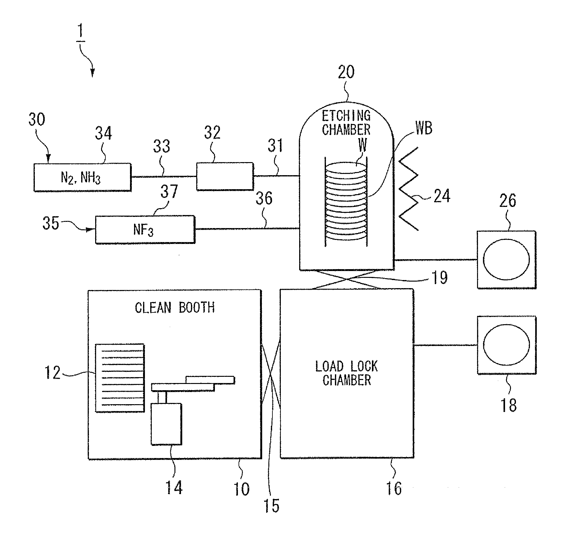
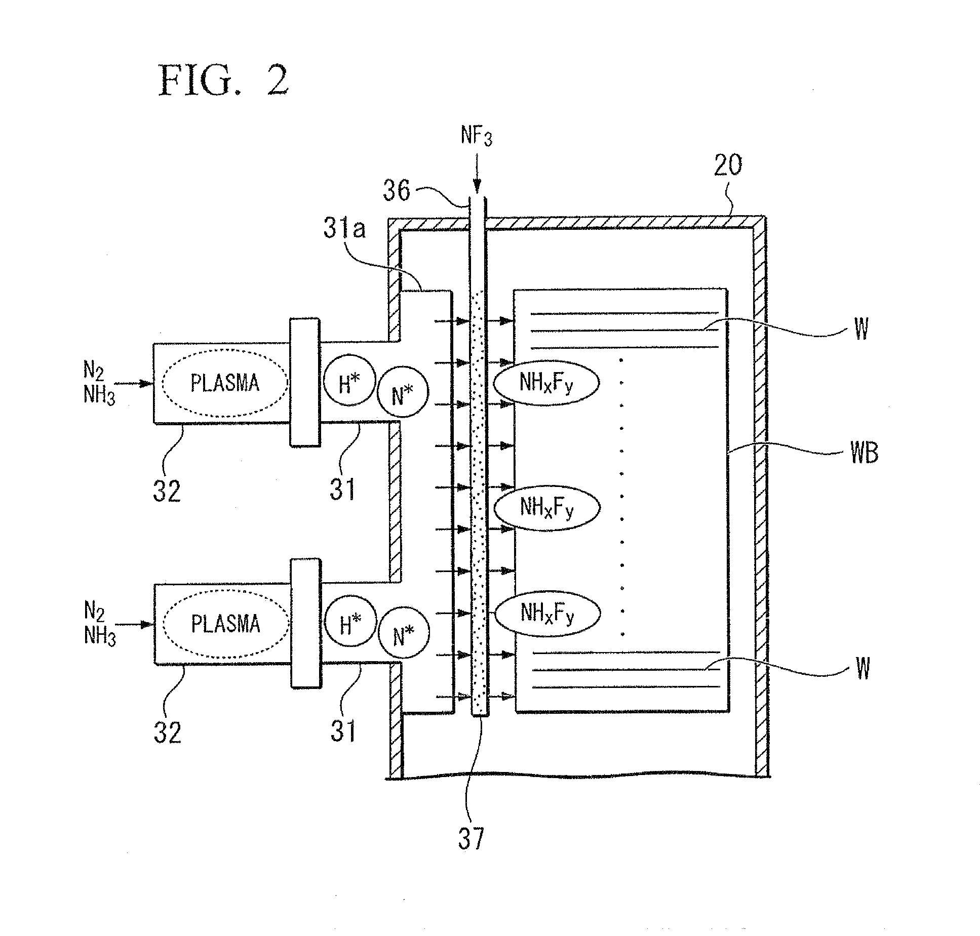
[0053]In the film forming method according to the first embodiment, the first process of converting a natural oxide film into a volatile material and the second process of evaporating the volatile material are performed by a natural oxide film removing apparatus shown in FIG. 1
[0054]A natural oxide film removing apparatus 1 shown in FIG. 1 includes a clean booth 10, a load lock chamber 16, and an etching chamber 20 as main components, and gate valves 15 and 19 are provided among the chambers. A substrate transport robot 14 is provided in the c...
second embodiment
Film Forming Apparatus
[0079]Next, a second embodiment of the present invention will be described.
[0080]FIG. 6 is a diagram schematically the structure of a film forming apparatus according to the second embodiment. In the first embodiment, the natural oxide film removing apparatus including the etching chamber and the SiGe growing apparatus including the SiGe growing chamber are individually used. However, a film forming apparatus 3 according to the second embodiment includes an etching chamber (first processing chamber) 20, a SiGe growing chamber (second processing chamber) 40, and a substrate transport chamber 16 that transports a silicon substrate W from the etching chamber 20 to the SiGe growing chamber 40 in a controlled atmosphere. In the second embodiment, a detailed description of the same components as those in the first embodiment will be omitted.
[0081]The film forming apparatus 3 includes the etching chamber 20 and the SiGe growing chamber 40 in addition to the clean boot...
first modification
(First Modification)
[0095]FIG. 8 is a diagram schematically illustrating the structure of a film forming apparatus according to a first modification of the second embodiment. In the second embodiment, the etching chamber including the reactant gas supply unit and the heater is used. However, the film forming apparatus according to the first modification differs from that according to the second embodiment in that it includes a first etching chamber 20a having a reactant gas supply unit and a second etching chamber 20b having a heater. In the first modification, a detailed description of the same components as those in the first embodiment or the second embodiment will be omitted.
[0096]A film forming apparatus 4 according to the first modification includes the first etching chamber (first processing chamber) 20a, the second etching chamber (second processing chamber) 20b, and the SiGe growing chamber (third processing chamber) 40 in addition to the clean booth 10 and the load lock ch...
PUM
| Property | Measurement | Unit |
|---|---|---|
| Temperature | aaaaa | aaaaa |
| Volatility | aaaaa | aaaaa |
Abstract
Description
Claims
Application Information