Film forming apparatus and method

a film forming and film technology, applied in the direction of coatings, chemical vapor deposition coatings, semiconductor devices, etc., can solve the problems of reducing power utilization efficiency, difficult to use induction heating for film forming apparatus, and high thermal decomposition temperature of source gas, so as to achieve stable film formation

Inactive Publication Date: 2010-02-25
TOKYO ELECTRON LTD
View PDF11 Cites 12 Cited by
  • Summary
  • Abstract
  • Description
  • Claims
  • Application Information

AI Technical Summary

Benefits of technology

[0028]In accordance with the present invention, it is possible to provide a film forming apparatus and method which can perform stable film formation by decomposing a film forming gas having a high decomposition temperature.

Problems solved by technology

However, a source gas may have a high thermal decomposition temperature.
In such a case, it is required to increase the temperature of the substrate to be higher than the thermal decomposition temperature, which makes it difficult to use the induction heating for a film forming apparatus.
For example, in the induction heating using a coil, a power conversion efficiency, i.e., the ratio of thermal energy for heating the substrate to input electric power, is low, resulting in the reduced power utilization efficiency.
Accordingly, especially when decomposing a film forming gas having a high thermal decomposition temperature, the amount of input electric power for induction heating increases, and the cost for film formation increases.
Further, in order to heat a substrate to a high temperature, a high frequency electric power supply for induction heating needs to be scaled up and, also, a high frequency shielding structure has to be scaled up and complex, resulting in a scaled up and complicated film forming apparatus.
One of the reasons for the deterioration of the conversion efficiency of the induction heating is that it is difficult to install a coil used for the induction heating near a substrate.
For example, the coil for the induction heating is installed outside a processing chamber made of a material having a low dielectric loss, e.g., quartz or the like, and thus cannot be installed near the substrate provided inside the corresponding processing chamber.
Moreover, the heater is provided inside the processing chamber which is maintained in a vacuum state, thereby causing the degassing or the thermal decomposition (sublimation) of the heater itself.

Method used


Image

  • Film forming apparatus and method
  • Film forming apparatus and method
  • Film forming apparatus and method

Examples


first embodiment

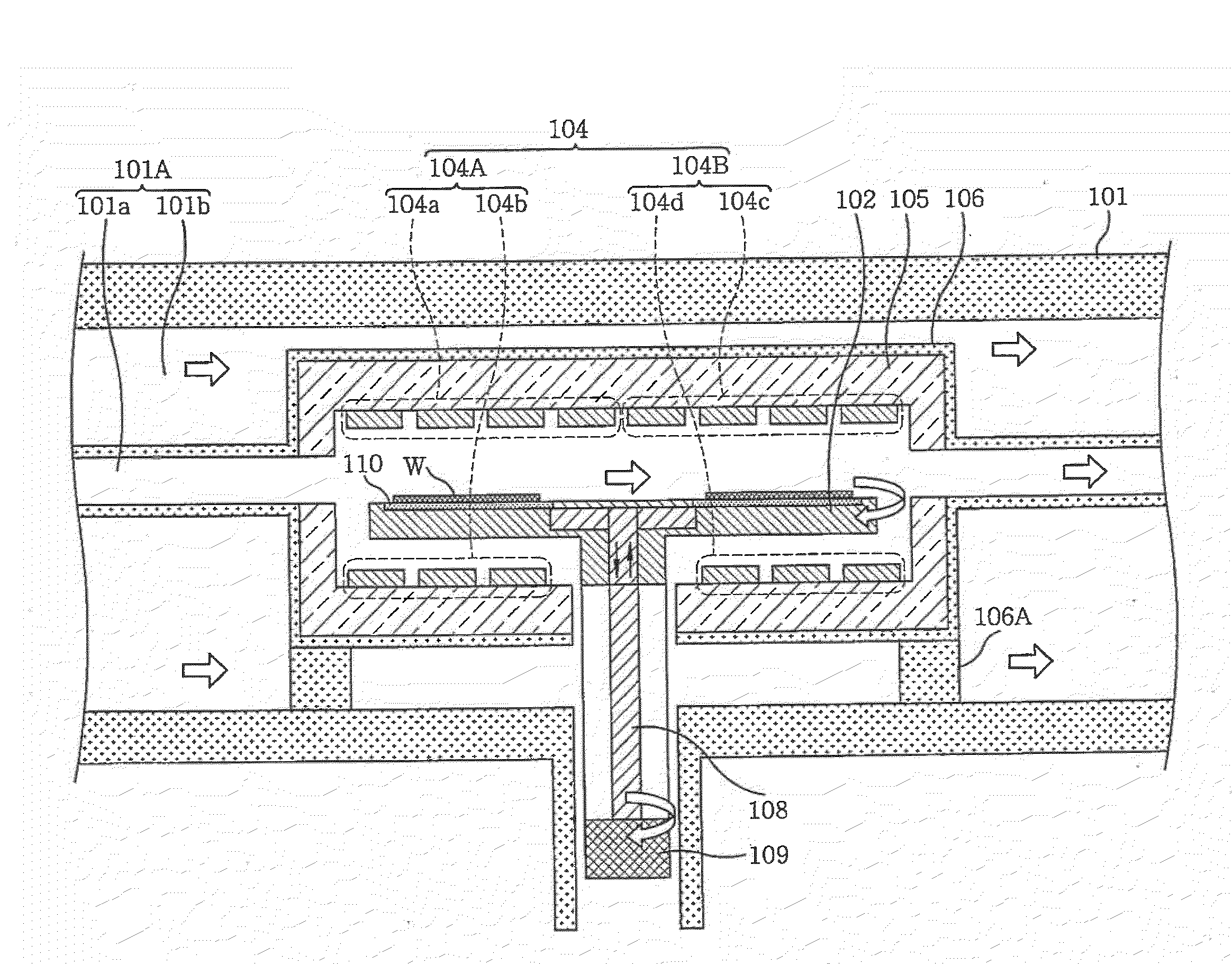
[0055]FIG. 3 schematically illustrates a film forming apparatus 100 in accordance with a first embodiment of the present invention. Referring to FIG. 3, the film forming apparatus 100 has a substantially cuboid-shaped (substantially housing-shaped) processing chamber 101 inside which a vacuum space 101A is defined.

[0056]Provided in the vacuum space 101A is a substrate supporting unit for supporting a substrate (the substrate and the substrate supporting unit not being shown in FIG. 3, but illustrated in detail in FIG. 4). A semiconductor film grows on the substrate supported by the substrate supporting unit. Further, an inner structure of the vacuum space 101A is not shown in FIG. 3, but is illustrated in detail in FIG. 4 and the drawings thereafter.

[0057]Besides, the processing chamber 101 is connected with a gas exhaust unit 114, e.g., a vacuum pump or the like, and a gas exhaust line 112, a pressure control unit 113 with, e.g., a variable conductance valve being provided in the g...


PUM

PropertyMeasurementUnit
temperatureaaaaaaaaaa
decomposition temperatureaaaaaaaaaa

Abstract

A film forming apparatus includes a processing chamber inside which a vacuum space is maintained and to which a film forming gas is supplied, a substrate supporting unit which is disposed inside the processing chamber and supports a substrate, and a heater which is made of a compound material comprising a high-melting point metal and carbon, is disposed inside the processing chamber, and heats the substrate.

Description

FIELD OF THE INVENTION[0001]The present invention relates to a film forming apparatus and method which performs film formation on a substrate by using a heater.BACKGROUND OF THE INVENTION[0002]An epitaxial growth method can grow on a crystal substrate a single crystal having a crystal orientation identical to that of the crystal substrate, and thus is used in various fields.[0003]For example, the following Patent Documents 1 and 2 describe methods for manufacturing a silicon wafer by an epitaxial growth method of Si.[0004]In the above epitaxial growth method, it is preferable that a substrate, on which a predetermined film grows, is heated to a temperature higher than the decomposition temperature of a source gas so that the source gas can be thermally decomposed. Accordingly, induction heating using a coil may be used to heat the substrate for example.[0005]Patent Document 1: Japanese Patent Laid-open Application No. H9-232275[0006]Patent Document 2: Japanese Patent Laid-open Appli...

Claims


Application Information

Patent Timeline
Patent Type & Authority Applications(United States)
IPC IPC(8): C23C16/44C23C16/22
CPCC23C16/4584C23C16/46H01L29/66068H01L21/0262H01L21/67115H01L21/02529C23C16/32H01L21/205
Inventor MORISAKI, EISUKEKOBAYASHI, HIROKATSUHARASHIMA, MASAYUKI
Owner TOKYO ELECTRON LTD
Why Eureka
Try Eureka