Organic Thin Film Transistors

Inactive Publication Date: 2010-03-04
CAMBRIDGE DISPLAY TECH LTD +1
View PDF10 Cites 27 Cited by
  • Summary
  • Abstract
  • Description
  • Claims
  • Application Information

AI Technical Summary

Benefits of technology

[0027]The bottom-gate arrangement of the fourth aspect of the invention may serve to minimise parasitic c

Problems solved by technology

One problem with organic thin film transistors is parasitic gate capacitance and gate leakage to the source and drain.
However, if the thickness of the gate insulating material is increased adjacent the channel region, then a larger voltage will be required to turn on the transistor.
One possible problem with both the aforementioned arrangements is that they require extra dielectric material to be deposited over the organic semi-conductive layer which may damage the organic semi-conductive layer.
Another possible problem with both the aforementioned arrangements is that it is difficult to align all the overlying layers in the device, such as alignment of the gate with the channel region between the source an

Method used


Image

  • Organic Thin Film Transistors
  • Organic Thin Film Transistors
  • Organic Thin Film Transistors

Examples


Embodiment Construction

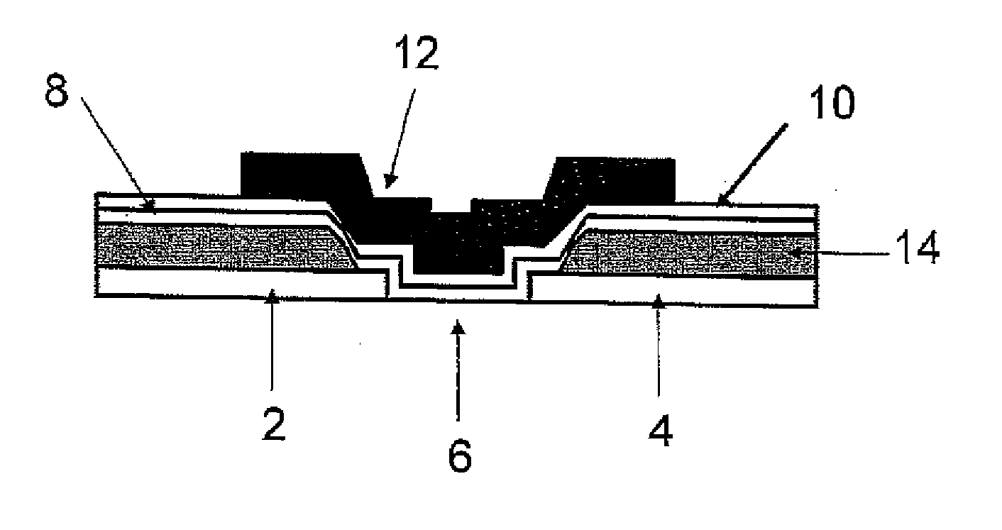
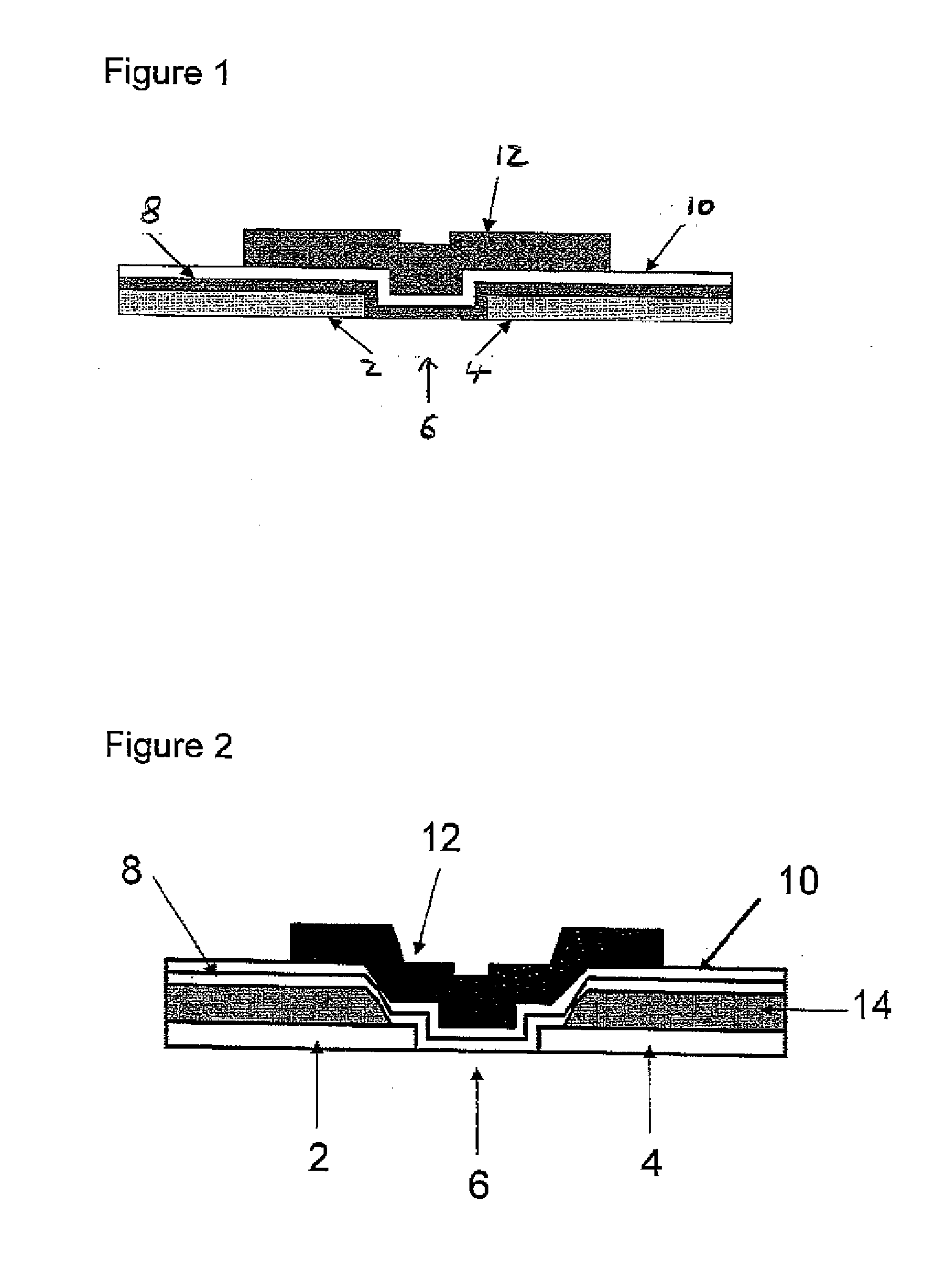
[0040]FIG. 2 shows a top-gate organic thin film transistor structure according to an embodiment of the present invention. The transistor is of the insulated gate field-effect type.

[0041]The transistor has a similar structure to that illustrated in FIG. 1 and previously described in the background section. For reasons of clarity, the same reference numerals have been used as in FIG. 1 for common layers. The important difference is that in the arrangement illustrated in FIG. 2, a layer of insulating material 14 is disposed over the source and drain 2, 4 forming a well. This layer isolates the peripheral areas of the overlying gate electrode 12 from the source and drain 2, 4 so as to minimise capacitance and gate leakage to the source and drain. The insulation layer 14 also serves to form a well in which the other layers of the organic thin film transistor can be deposited to enhance alignment.

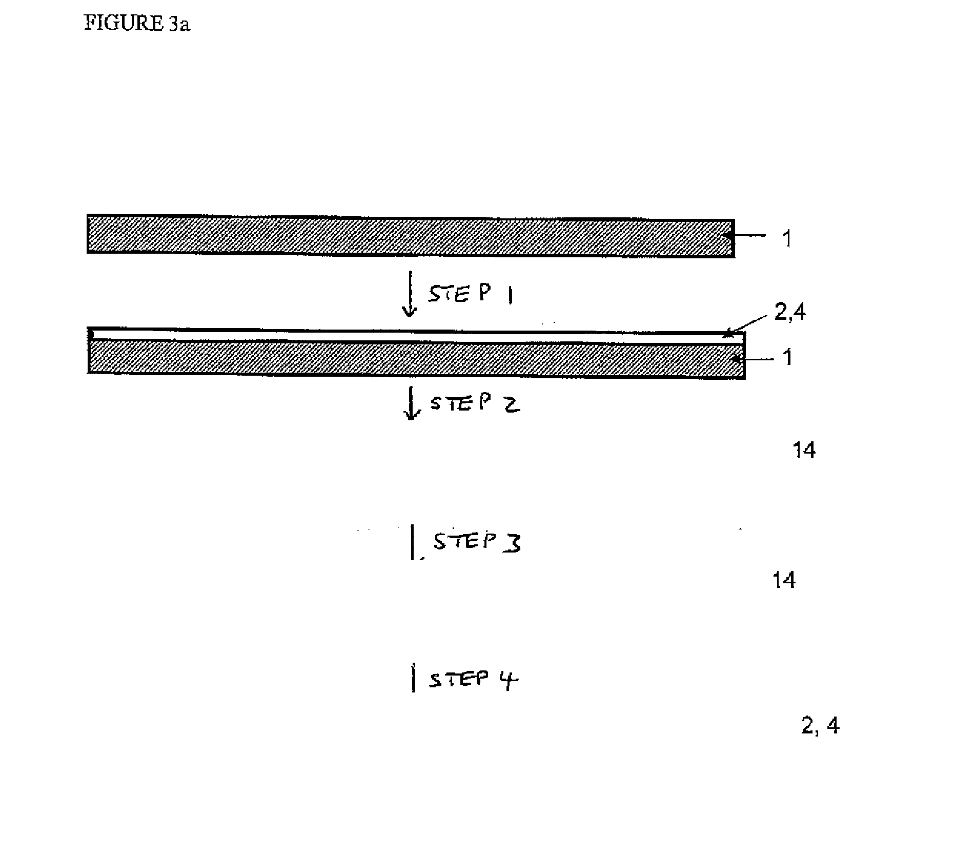
[0042]FIG. 3a illustrates the method steps involved in forming the organic thin film transist...


PUM


Abstract

An organic thin film transistor comprising: a substrate; a source electrode and a drain electrode defining a channel; a layer of insulating material disposed over the source and drain electrodes; a layer of organic semi-conductive material extending across the channel; a layer of dielectric material; and a gate electrode disposed over the layer of dielectric material.

Description

FIELD OF INVENTION[0001]The present invention relates to organic thin film transistors.BACKGROUND OF THE INVENTION[0002]Transistors can be divided into two main types: bipolar junction transistors and field-effect transistors. Both types share a common structure comprising three electrodes with a semi-conductive material disposed therebetween in a channel region. The three electrodes of a bipolar junction transistor are known as the emitter, collector and base, whereas in a field-effect transistor the three electrodes are known as the source, drain and gate. Bipolar junction transistors may be described as current-operated devices as the current between the emitter and collector is controlled by the current flowing between the base and emitter. In contrast, field-effect transistors may be described as voltage-operated devices as the current flowing between source and drain is controlled by the voltage between the gate and the source.[0003]Transistors can also be classified as p-type...

Claims


Application Information

Patent Timeline
IPC IPC(8): H01L51/10H01L51/40H01L21/336H01L29/786
CPCH01L51/0541H01L51/0005H10K71/135H10K10/464H10K10/474H10K10/84
Inventor HOTTA, SADAYOSHIBURROUGHES, JEREMY HENLEYWHITING, GREGORY LEWIS
Owner CAMBRIDGE DISPLAY TECH LTD
Why Eureka
Try Eureka