Semiconductor device and fabrication method for the same
a technology of semiconductor devices and fabrication methods, which is applied in the direction of semiconductor devices, basic electric elements, electrical appliances, etc., can solve the problems of reducing affecting the performance of semiconductor devices, and affecting the reliability of power semiconductor devices, etc., to achieve high reliability, high power, and high performance.
- Summary
- Abstract
- Description
- Claims
- Application Information
AI Technical Summary
Benefits of technology
Problems solved by technology
Method used
Image

Examples
first embodiment
(Element Structure)
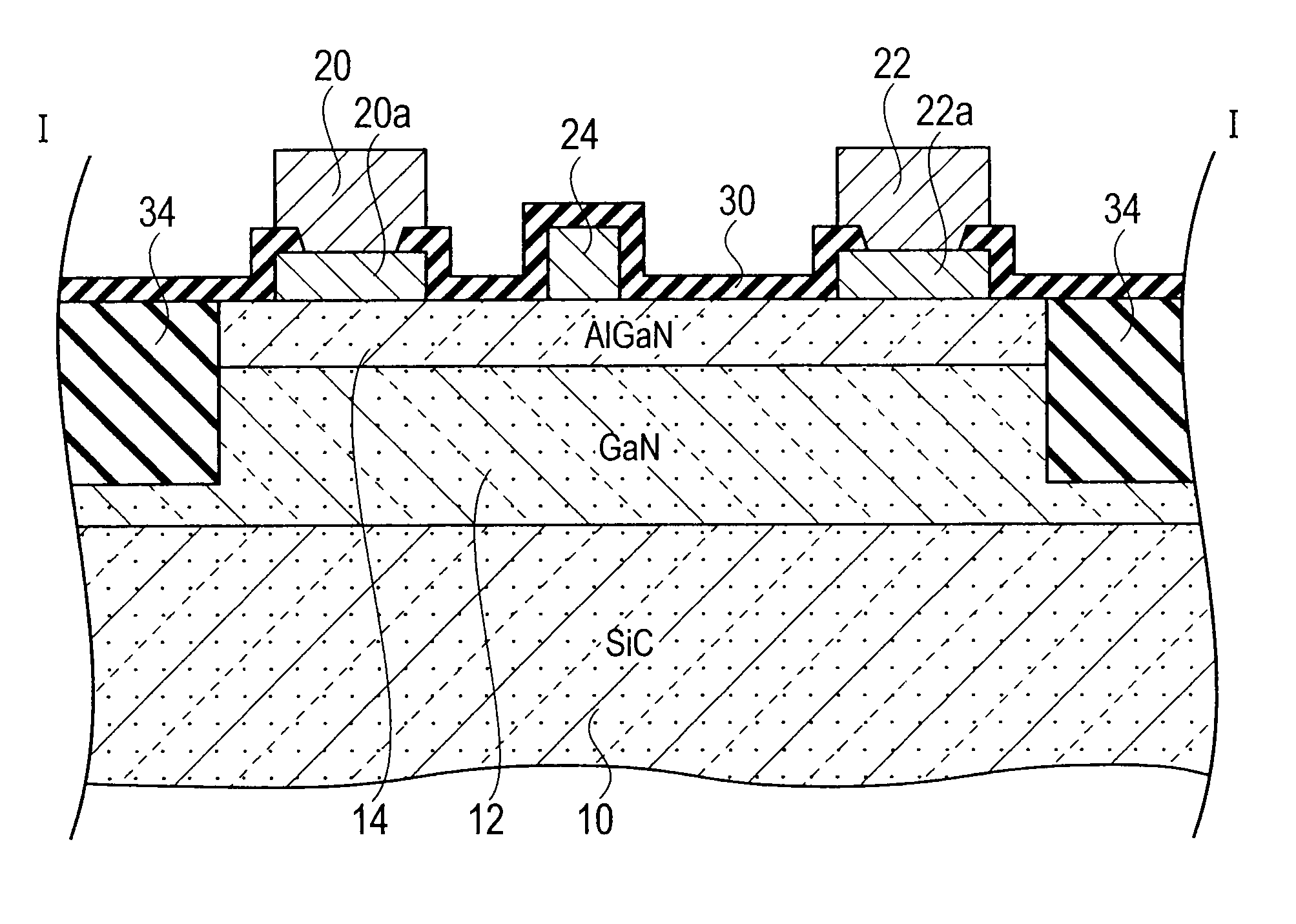
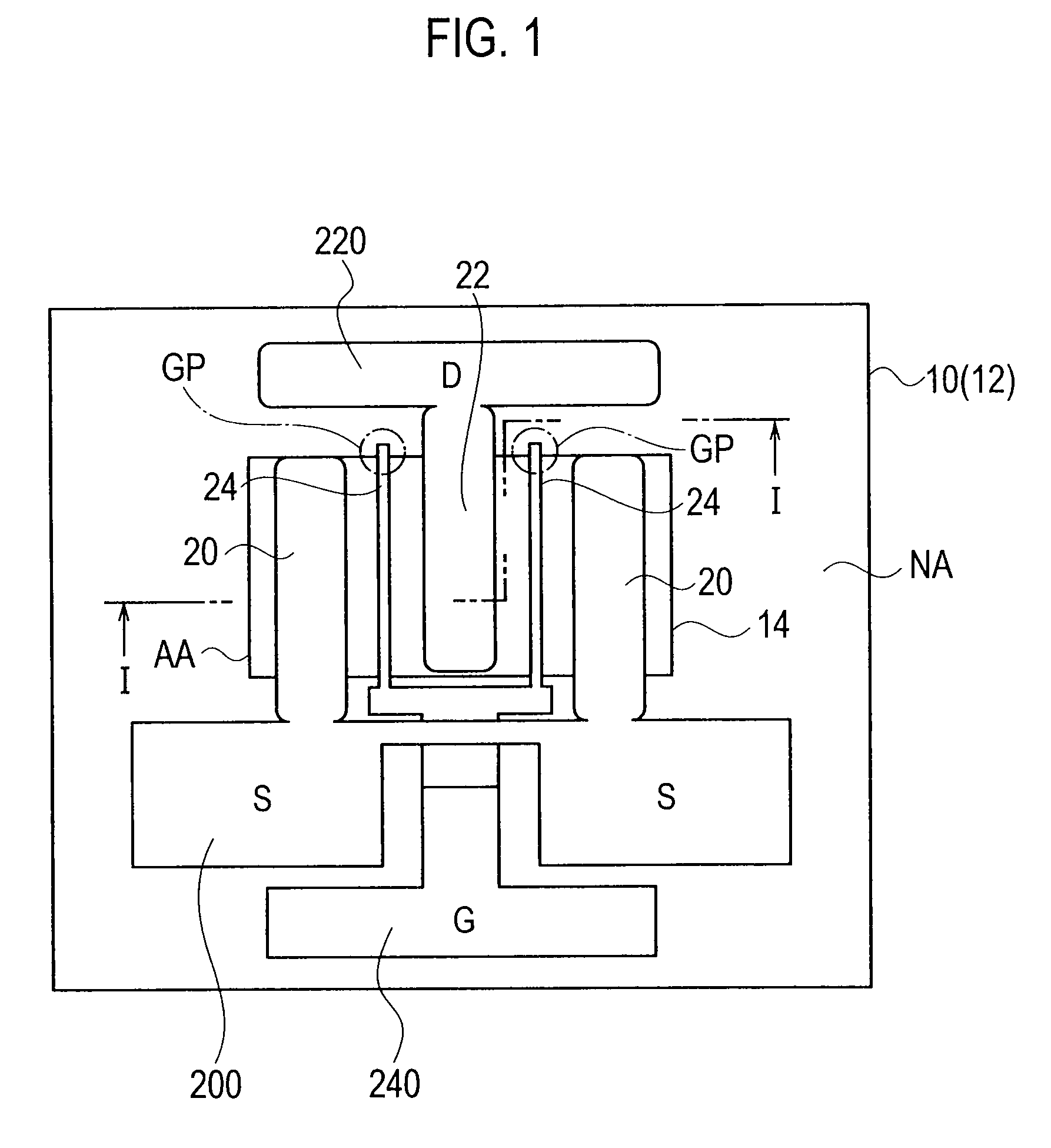
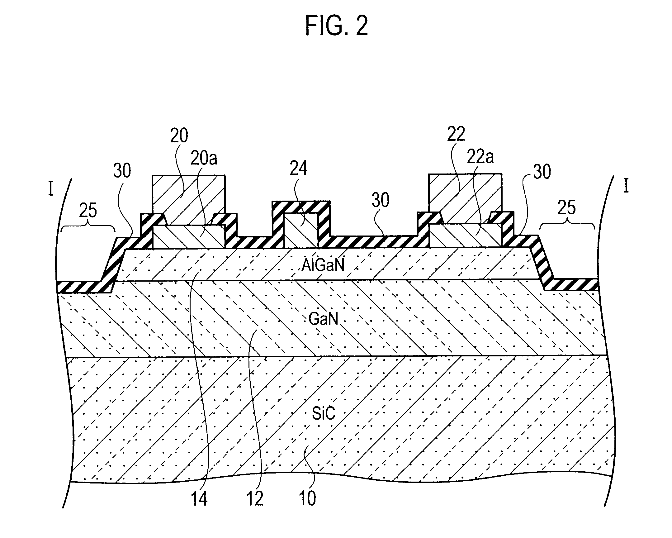
[0047]A schematic plane pattern configuration of a semiconductor device according to a first embodiment of the present invention is expressed as shown in FIG. 3. Moreover, a schematic section structure taken in the line I-I of FIG. 3 is expressed as shown in FIG. 4, and a schematic section structure taken in the line II-II of FIG. 3 is expressed as shown in FIG. 5.
[0048]As shown in FIG. 3 to FIG. 5, the semiconductor device according to the first embodiment includes a substrate 10; a nitride based compound semiconductor layer 12 placed on the substrate 10; an active area AA which is placed on the nitride based compound semiconductor layer 12, and is composed of the aluminum gallium nitride layer (AlxGa1-xN) (where 0.114; an isolation region 34 which performs isolation of the active area AA mutually; a trench region 28a formed by etching for a part of previous arrangement to the gate electrode 24; and a gate electrode 24, a source electrode 20, and a drain electrod...
second embodiment
(Element Structure)
[0072]An overall schematic plane pattern configuration of a semiconductor device according to a second embodiment is expressed as shown in FIG. 7. Moreover, the enlarged drawing of the part A of FIG. 7 is expressed as shown in FIG. 8. Since the fundamental element section structure is the same as that of FIG. 4 to FIG. 5 shown in the first embodiment, the description of each layer is omitted.
[0073]In the semiconductor device according to the second embodiment, an electrode pattern assignment for high power and the trench region 38a formed under the gate electrode 24 are provided.
[0074]As shown in FIG. 4 to FIG. 5 and FIG. 7 to FIG. 8, the overall configuration of the semiconductor device according to the second embodiment includes a substrate 10; a nitride based compound semiconductor layer 12 placed on the substrate 10; an active area AA which is placed on the nitride based compound semiconductor layer 12, and is composed of the aluminum gallium nitride layer (Al...
third embodiment
(Element Structure)
[0095]The schematic plane pattern configuration of a semiconductor device according to a third embodiment of the present invention is expressed as shown in FIG. 10. Moreover, the schematic section structure taken in the line III-III of FIG. 10 is expressed as shown in FIG. 11 or FIG. 12. The example of FIG. 11 is a section structure which forms an isolation region 34 acting as a non-active area NA by using ion implantation technology, and the example of FIG. 12 is a section structure which forms an isolation region 25 acting as a non-active area NA by using mesa etching technology.
[0096]As shown in FIG. 10 to FIG. 12, the semiconductor device according to the third embodiment includes a substrate 10; a nitride based compound semiconductor layer 12 placed on the substrate 10; an active area AA which is placed on the nitride based compound semiconductor layer 12, and is composed of the aluminum gallium nitride layer (AlxGa1-xN) (where 0.114; an isolation regions (34...
PUM
 Abstract
Description
Claims
Application Information
 - R&D
- Intellectual Property
- Life Sciences
- Materials
- Tech Scout
- Unparalleled Data Quality
- Higher Quality Content
- 60% Fewer Hallucinations
Browse by: Latest US Patents, China's latest patents, Technical Efficacy Thesaurus, Application Domain, Technology Topic, Popular Technical Reports.
© 2025 PatSnap. All rights reserved.Legal|Privacy policy|Modern Slavery Act Transparency Statement|Sitemap|About US| Contact US: help@patsnap.com