Packaging substrate with embedded semiconductor component and method for fabricating the same

a technology of embedded semiconductors and packaging substrates, which is applied in the direction of printed circuit components, electrical apparatus construction details, printed circuit non-printed electric components association, etc., can solve the problems of easy damage to semiconductor chips, low speed, and failure of electrical connections, so as to avoid conventional drawbacks, increase alignment precision, and prevent semiconductor chips efficiently

Active Publication Date: 2010-03-04
UNIMICRON TECH CORP
View PDF4 Cites 17 Cited by
  • Summary
  • Abstract
  • Description
  • Claims
  • Application Information

AI Technical Summary

Benefits of technology

[0009]In view of the above drawbacks of the prior art, the present invention provides a packaging substrate with an embedded semiconductor component and a method for fabricating the same so as to increase the precision of alignment between electrical connection elements and thereby enhance quality of electrical connection.
[0010]The present invention further provides a packaging substrate with an embedded semiconductor component and a method for fabricating the same so as to prevent a semiconductor chip from positional deviation which might otherwise occur due to an external force.
[0023]According to the present invention, the semiconductor chip is first fixed in position to the assisting layer and then both the assisting layer and the semiconductor chip are coupled with the first dielectric layer. Thus, the present invention dispenses with heat lamination by dielectric layer in a later circuit forming process and thereby efficiently prevents the semiconductor chip from positional deviation which might otherwise occur under an external force.
[0024]Further, before the semiconductor chip and the assisting layer are coupled with the first dielectric layer, the bumps on the electrode pads of the semiconductor chip are aligned and attached to the filling material in the apertures of the assisting layer. Thus, the conductive vias formed later by removing the bumps and the filling material in the apertures electrically connect the electrode pads to the first wiring layer, and the electrode pads can further be aligned with an external circuit through the conductive lands of the first wiring layer formed right on the first conductive vias, thereby increasing the precision of alignment between the electrode pads and the external circuit.
[0025]Meanwhile, after the semiconductor chip and the assisting layer are coupled with the first dielectric layer, vias can be formed by removing bumps formed on the electrode pads and at the same time removing the filling material in the corresponding apertures. Therefore, the present invention dispenses with a conventional laser processing and accordingly avoids the conventional drawbacks caused by the laser processing.

Problems solved by technology

Meanwhile, an alignment error may occur during the laser processing for forming the vias 141, thus resulting an alignment deviation between the conductive vias 16 and the electrode pads 121 and even causing failure of the electrical connection therebetween.
In addition, the laser processing requires a high cost, has a low speed and is easy to damage the semiconductor chip 12.

Method used


Image

  • Packaging substrate with embedded semiconductor component and method for fabricating the same
  • Packaging substrate with embedded semiconductor component and method for fabricating the same
  • Packaging substrate with embedded semiconductor component and method for fabricating the same

Examples


first embodiment

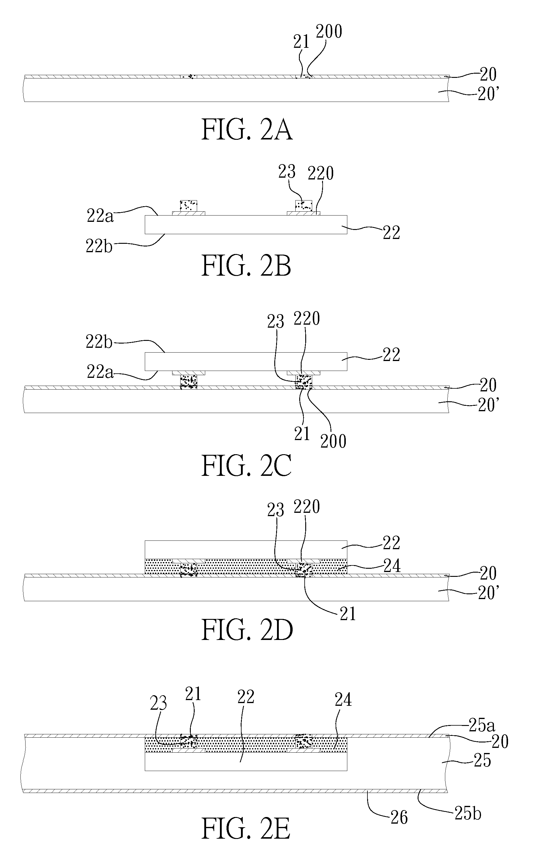
[0030]FIGS. 2A to 2M are sectional views showing a method for fabricating a packaging substrate with an embedded semiconductor component according to a first embodiment of the present invention.

[0031]Referring to FIG. 2A, a carrier board 20′ is provided, and an assisting layer 20 made of a metal material is formed on the carrier board 20′, wherein the assisting layer 20 has a plurality of apertures 200 each filled with a filling material 21. In the present embodiment, the assisting layer 20 is made of a copper foil.

[0032]Referring to FIG. 2B, a semiconductor chip 22 has an active surface 22a with a plurality of electrode pads 220 thereon and an opposite inactive surface 22b. A plurality of bumps 23 are formed on the electrode pads 230, respectively.

[0033]Referring to FIG. 2C, the bumps 23 correspond in position to the apertures 200, respectively, and are attached to the filling material 21 in the apertures 200, thereby allowing the semiconductor chip 22 to be coupled to the assistin...

second embodiment

[0043]FIGS. 3A to 3J are sectional views showing a method for fabricating a packaging substrate with an embedded semiconductor component according to a second embodiment of the present invention. In the present embodiment, the assisting layer 20 is made of a dielectric material.

[0044]Referring to FIG. 3A, a carrier board 20′ is provided, and an assisting layer 20 made of a dielectric material is formed on the carrier board 20′, wherein the assisting layer 20 has a plurality of apertures 200 each filled with a filling material 21.

[0045]Referring to FIGS. 3B to 3D, a plurality of bumps 23 are formed on the electrode pads 220 of the semiconductor chip 22, respectively. The bumps 23 correspond in position to the apertures 200, respectively, and are attached to the filling material 21 in the apertures 200, so as for the semiconductor chip 22 to be fixed in position to the assisting layer 20. Further, an adhesive member 24 is filled between the assisting layer 20 and the semiconductor chi...


PUM

PropertyMeasurementUnit
conductiveaaaaaaaaaa
electricallyaaaaaaaaaa
sizeaaaaaaaaaa

Abstract

A packaging substrate with an embedded semiconductor component and a method of fabricating the same are provided, including: fixing a semiconductor chip with electrode pads to an assisting layer with apertures through an adhesive member, wherein each of the electrode pads has a bump formed thereon, each of the apertures is filled with a filling material, and the bumps correspond to the apertures, respectively; forming a first dielectric layer on the assisting layer to encapsulate the semiconductor chip; removing the bumps and the filling material to form vias; and forming a first wiring layer on the first dielectric layer and forming first conductive vias in the vias to provide electrical connections between the electrode pads and the first wiring layer, wherein the first wiring layer comprises a plurality of conductive lands formed right on the first conductive vias, respectively.

Description

BACKGROUND OF THE INVENTION[0001]1. Field of the Invention[0002]The present invention relates generally to packaging substrates and methods for fabricating the same, and more particularly to a packaging substrate with an embedded semiconductor component and a method for fabricating the same.[0003]2. Description of Related Art[0004]In addition to conventional wire bonding packages, the electronic industry developed, thanks to ever-evolving semiconductor packaging technology, various semiconductor device packages. For example, an IC semiconductor chip can be directly embedded in a packaging substrate and electrically integrated therewith so as to reduce the overall size of the semiconductor device and enhance the electrical function thereof. Such a package type has become a mainstream.[0005]FIGS. 1A to 1D shows a method for fabricating a conventional package structure with an embedded semiconductor component. Referring to FIG. 1A, a first carrier board 10 having a first surface 10a an...

Claims


Application Information

Patent Timeline
Patent Type & Authority Applications(United States)
IPC IPC(8): H05K1/18H01L21/56
CPCH01L21/486H01L2924/014H01L23/5389H01L24/24H01L24/82H01L2224/24227H01L2924/01029H05K1/185H05K1/188H05K3/20H05K3/305H05K3/421H05K3/4602H05K2201/10674H05K2203/1469H05K2203/308H01L2924/01033H01L23/49827H01L21/568H01L2224/04105H01L2924/12042Y10T29/49146
Inventor ZENG, ZHAO CHONG
Owner UNIMICRON TECH CORP
Why Eureka
Try Eureka