Photoelectric conversion device and method of manufacturing the same

a technology of photoelectric conversion and conversion device, which is applied in the direction of semiconductor/solid-state device manufacturing, semiconductor devices, electrical apparatus, etc., can solve the problems of low spatial resolution, lack of immediacy, and disadvantages of upsizing limits, and achieve the effect of suppressing leakage curren

Active Publication Date: 2010-03-11
TRIVALE TECH
View PDF3 Cites 44 Cited by
  • Summary
  • Abstract
  • Description
  • Claims
  • Application Information

AI Technical Summary

Benefits of technology

[0015]According to the embodiments of the present invention described above, it is possible to provide a photoelectric conversion device that enables suppression of leakage current of a photodiode, and a method of manufacturing the same.

Problems solved by technology

Further, the X-ray film requires a processing procedure after taking images and thus has a disadvantage of lack of immediacy.
On the other hand, while the image pickup tube has a high sensitivity and is capable of taking moving images, it has a low spatial resolution.
Further, the image pickup tube is a vacuum device and thus has a disadvantage of limits on upsizing.
When forming a photodiode, the photodiode is damaged on its end face due to etching or the like of an amorphous silicon layer, which is a photoelectric conversion layer.
Therefore, damage recovery by H2 plasma processing cannot be performed on the photodiode disclosed in Japanese Unexamined Patent Application Publication No. 2000-101920.
This causes an increase in leakage current of the photodiode.
This is because a leakage path is created in the damaged part of the end face of the photodiode upon application of a reverse bias to the transparent conductive film when using the photodiode as a sensor.
However, in the structure disclosed in Japanese Unexamined Patent Application Publication No. 2007-165865, if the insulating film of a coating type is formed by exposure, a leakage path is created on the end face of the photodiode by an impurity contained in the insulating film.
On the other hand, if the insulating film is formed by deposition, not a coating type insulating film, damage is done to the semiconductor layer by dry etching upon making an opening in the insulating film.
As a result, rectification at the p-i interface is degraded, which causes an increase in leakage current.
As described above, in the photosensor using the photodiode disclosed in Japanese Unexamined Patent Application Publications Nos. 2000-101920 and 2007-165865, the S / N ratio is deteriorated due to an increase in leakage current.
It is thus impossible to obtain a suitable image with a small amount of incident light.

Method used


Image

  • Photoelectric conversion device and method of manufacturing the same
  • Photoelectric conversion device and method of manufacturing the same
  • Photoelectric conversion device and method of manufacturing the same

Examples


first embodiment

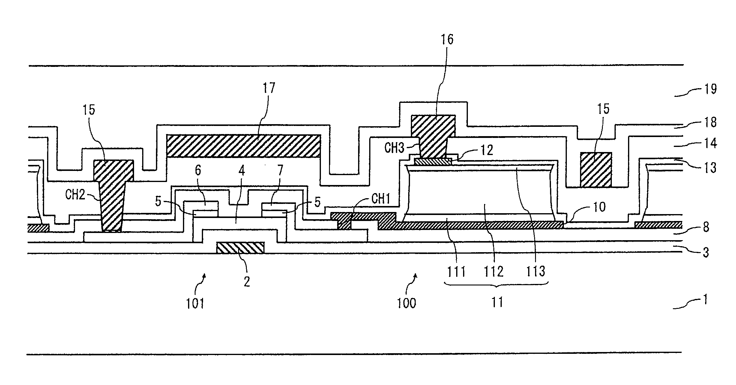
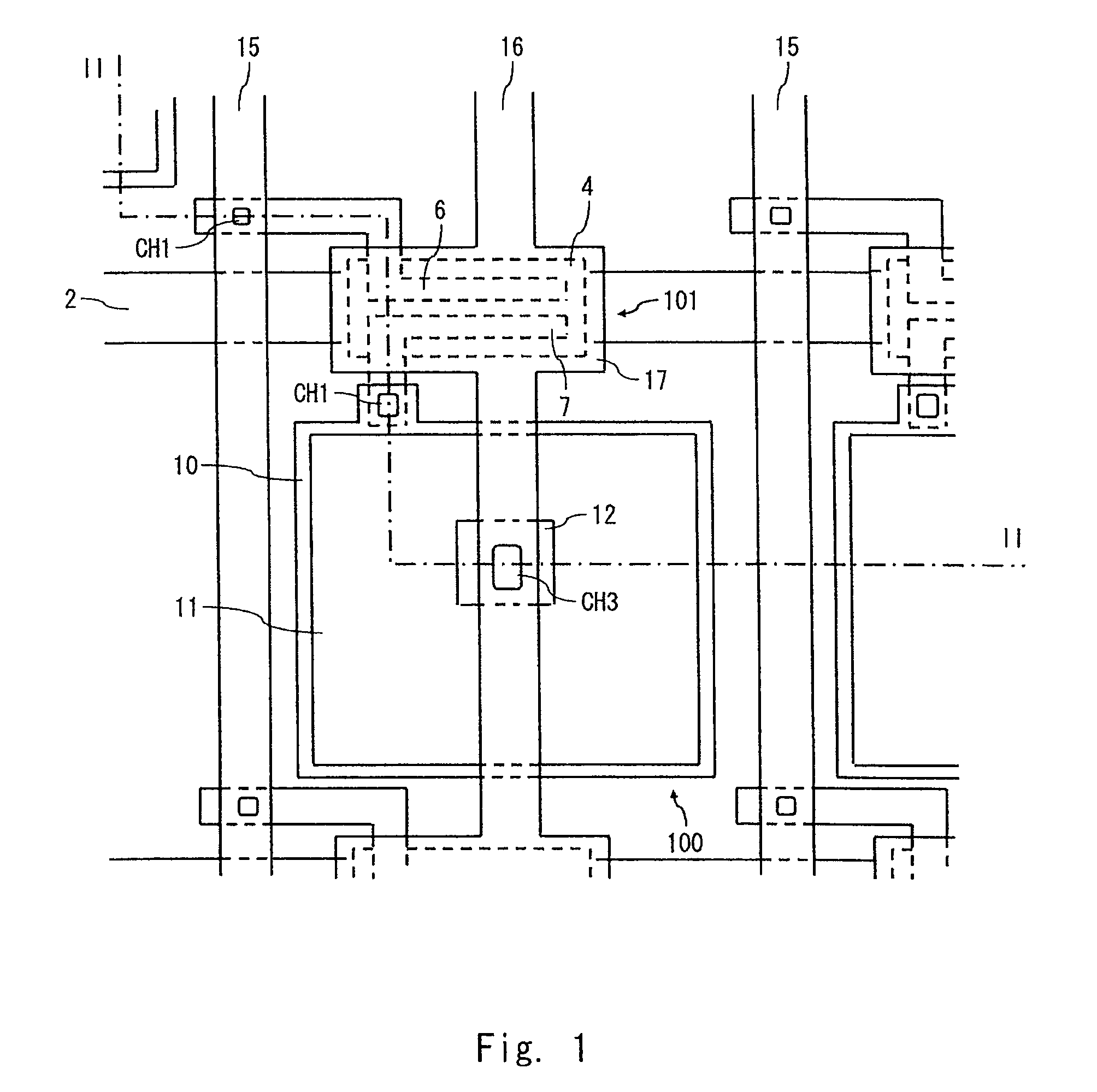
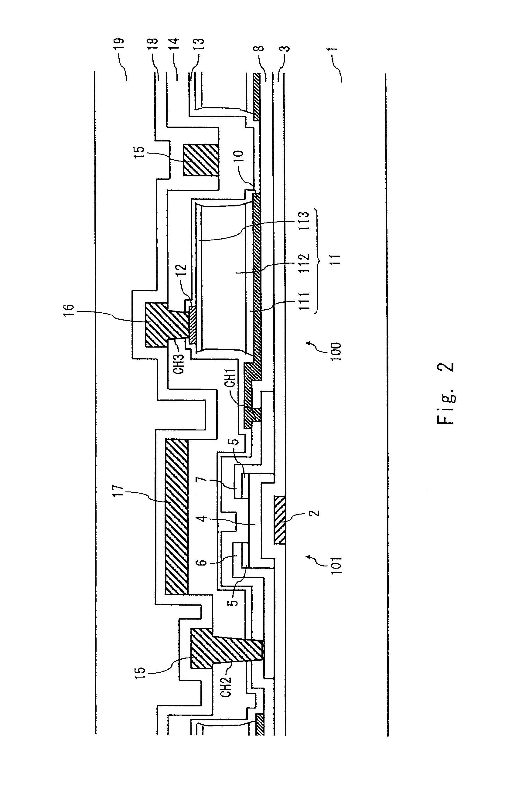
[0035]A photosensor (photoelectric conversion device) according to an embodiment of the present invention is described hereinafter with reference to FIGS. 1 and 2. FIG. 1 is a plan view showing a structure of an array substrate used in the photoelectric conversion device according to the first embodiment. FIG. 2 is a cross-sectional view along line II-II in FIG. 1.

[0036]On the array substrate, light receiving pixel areas are arranged in an array. FIG. 1 shows one of the light receiving pixel areas. In each light receiving pixel area, one photodiode 100 and one thin film transistor (TFT) 101 are placed as shown in FIGS. 1 and 2. Accordingly, on the array substrate, the photodiodes 100 and the TFTs 101 are arranged in an array.

[0037]Hereinafter, an area where the photodiodes 100 and the TFTs 101 are arranged in an array is referred to as an element area, and an area outside the element area is referred to as a peripheral area. For example, the element area is formed like a rectangular...

second embodiment

[0112]A photosensor (photoelectric conversion device) according to a second embodiment of the present invention is described hereinafter with reference to FIGS. 7 and 8. FIG. 7 is a plan view showing a structure of an array substrate used in the photoelectric conversion device according to the second embodiment. FIG. 8 is a cross-sectional view along line VIII-VIII in FIG. 7. In this embodiment, an upper electrode and a second passivation film that are different from those of the first embodiment are formed. The other structure is substantially the same as that of the first embodiment and thus not redundantly explained below.

[0113]Referring to FIGS. 7 and 8, in this embodiment, an upper electrode 12a made of a transparent conductive film is placed on the photoelectric conversion layer 11. The upper electrode 12a is formed in the most part on the photoelectric conversion layer 11. In this example, the upper electrode 12a that is slightly smaller than the photoelectric conversion laye...


PUM


Abstract

A photoelectric conversion device includes a thin film transistor that is placed on a substrate, a photodiode that is connected to a drain electrode of the thin film transistor and includes an upper electrode, a lower electrode and a photoelectric conversion layer placed between the upper and lower electrodes, a first interlayer insulating film that covers at least the upper electrode, a second interlayer insulating film that is placed in an upper layer of the first interlayer insulating film and covers the thin film transistor and the photodiode, and a line that is connected to the upper electrode through a contact hole disposed in the first interlayer insulating film and the second interlayer insulating film.

Description

BACKGROUND OF THE INVENTION[0001]1. Field of the Invention[0002]The present invention relates to a photoelectric conversion device and a method of manufacturing the same. Particularly, the present invention relates to a photoelectric conversion device that uses a substrate on which light receiving pixels including photodiodes and thin film transistors are arranged in an array, and a method of manufacturing the same.[0003]2. Description of Related Art[0004]A photosensor, which is a photoelectric conversion device, is a flat panel that includes a TFT array substrate on which a photodiode that photoelectrically converts visible light into an electric charge and a thin film transistor (TFT) are arranged. The photosensor is widely used in application to a contact image sensor, an X-ray imaging display device or the like. Particularly, a flat panel X-ray imaging display device (which is referred to hereinafter as a flat panel detector (FPD)) in which a scintillator that converts an X-ray ...

Claims


Application Information

Patent Timeline
Patent Type & Authority Applications(United States)
IPC IPC(8): H01L31/112H01L31/18
CPCH01L27/14603H01L27/14692H01L27/14663H01L27/14609
Inventor HAYASHI, MASAMIMIYAYAMA, TAKASHI
Owner TRIVALE TECH
Why Eureka
Try Eureka