System and Method for Packaged Memory

a technology of memory and system, applied in the field of semiconductor circuits, can solve the problems of increasing the demand for low power and compact electronic systems

Active Publication Date: 2010-03-18
POLARIS INNOVATIONS
View PDF2 Cites 108 Cited by
  • Summary
  • Abstract
  • Description
  • Claims
  • Application Information

AI Technical Summary

Problems solved by technology

As portable electronic devices become smaller, less expensive, and more power efficient, however, there has been an increased demand for low power and compact electronic systems in which DRAM is commonly used.

Method used


Image

  • System and Method for Packaged Memory
  • System and Method for Packaged Memory
  • System and Method for Packaged Memory

Examples


Embodiment Construction

[0014]The making and using of embodiments are discussed in detail below. It should be appreciated, however, that the present invention provides many applicable inventive concepts that may be embodied in a wide variety of specific contexts. The specific embodiments discussed are merely illustrative of specific ways to make and use the invention, and do not limit the scope of the invention.

[0015]The present invention will be described with respect to embodiments in a specific context, namely a system and method for a packaged DRAM memory. Embodiments of this invention may also be applied to other circuits and systems that require area and power efficient use of a memory device.

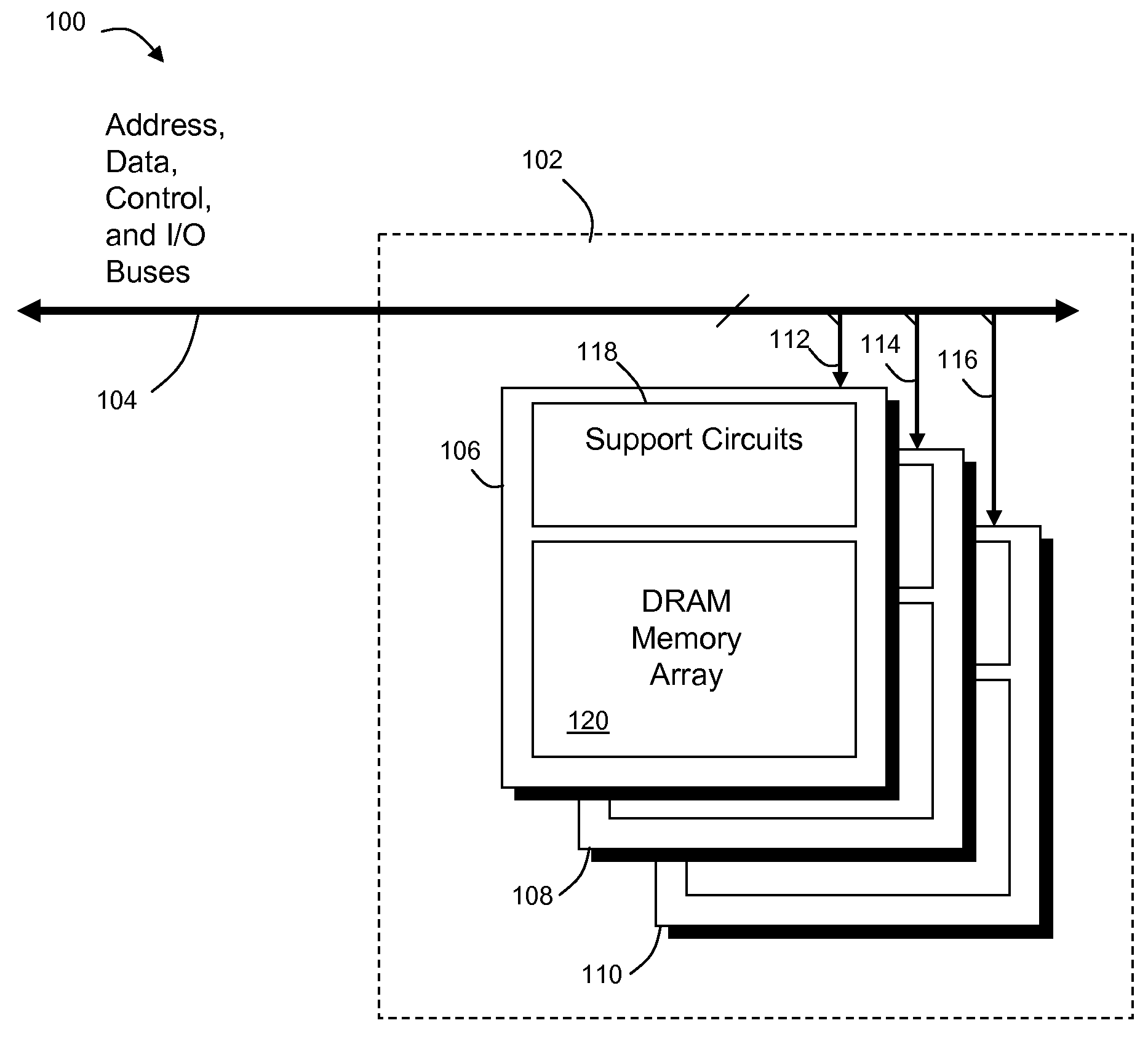
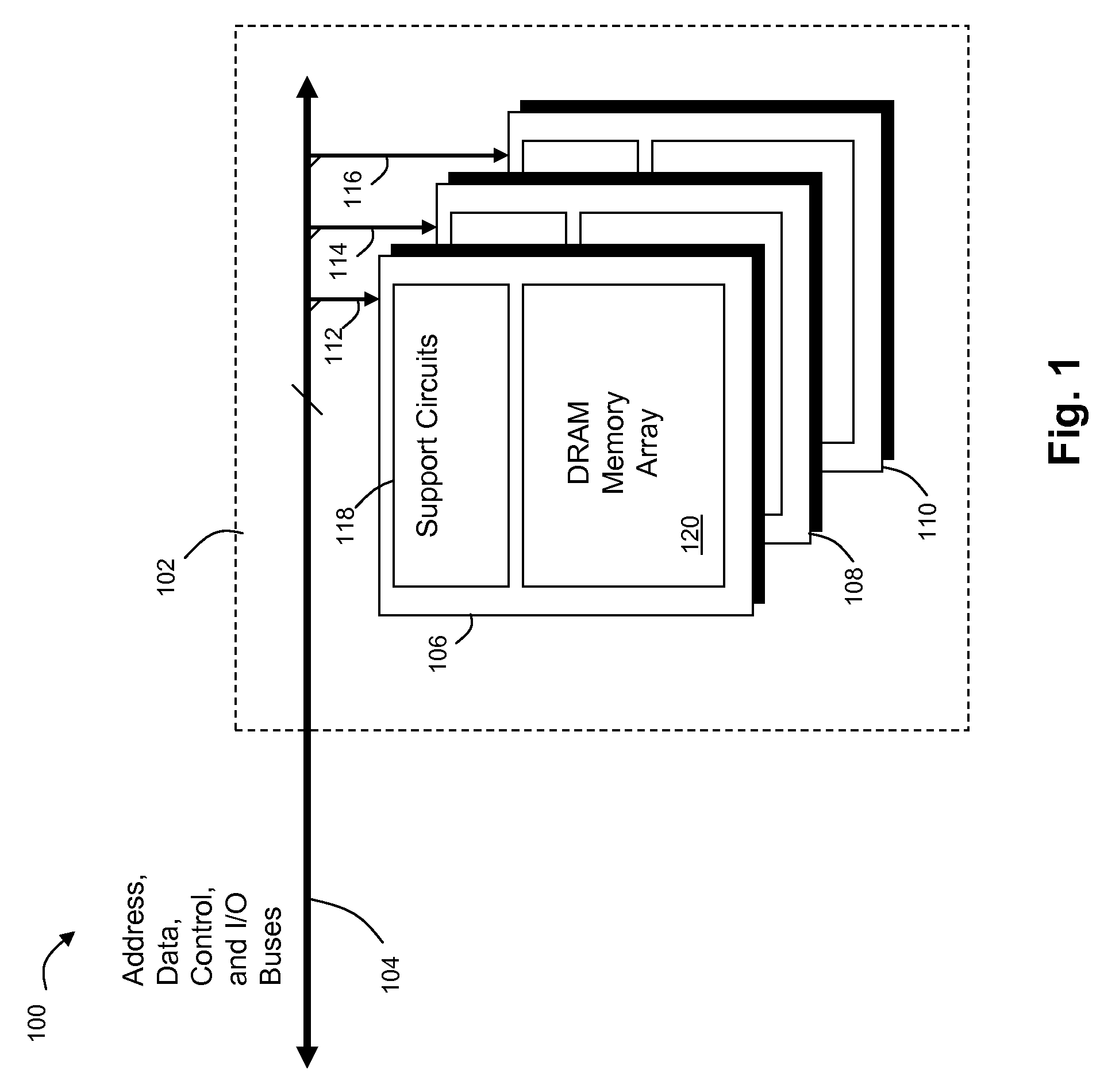
[0016]A known packaged memory system 100 is shown in FIG. 1, which shows DRAM memory integrated circuits (ICs) 106, 108 and 110 housed together in package 102. Generally DRAM ICs 106, 108 and 110 are stacked on top of each other within the same package. Three DRAM ICs 106, 108 and 110 are shown for simplicity of...


PUM


Abstract

In one embodiment, a memory system is disclosed. The memory system has at least one memory chip having an address and data interface coupled to an internal address and data bus, and a memory controller and interface chip also having a an address and data interface coupled to the address and data interface of the at least one memory chip via an internal address and data bus. The at least one memory chip, the memory controller and interface chip and the internal address and data bus are disposed within a common chip package. The memory controller and interface chip has an external interface configured to be coupled to a standard memory bus via external contacts of the common chip package.

Description

TECHNICAL FIELD[0001]This invention relates generally to semiconductor circuits, and more particularly to a system and method for packaged memory.BACKGROUND[0002]Semiconductor devices are used for integrated circuits in a variety of electrical and electronic applications, such as computers, cellular telephones, radios, and televisions. One particular type of semiconductor device is a semiconductor storage device, such as a random access memory (RAM) device. Many RAM devices include many storage cells arranged in a two-dimensional array with two sets of select lines, word lines and bit lines. An individual storage cell is selected by activating its word line and its bit line. RAM devices are considered “random access” because any memory cell in an array can be accessed directly if the row and column that intersect at that cell are known.[0003]A commonly used form of RAM is known as a dynamic RAM (DRAM) device. Dynamic random access memory has memory cells with a paired transistor and...

Claims


Application Information

Patent Timeline
Patent Type & Authority Applications(United States)
IPC IPC(8): G06F12/06
CPCG06F13/4243G11C5/02Y02B60/1235G11C5/063Y02B60/1228G11C5/04H01L24/50H01L2224/32225H01L2224/48091H01L2224/48227H01L2224/73265H01L2225/107H01L2924/14H01L2924/15311Y02D10/00H01L2224/32145H01L2924/00012H01L2924/00
Inventor BLANKENSHIP, DENNIS
Owner POLARIS INNOVATIONS
Why Eureka
Try Eureka