

Electronic component mounting structure
a technology of mounting structure and electronic components, applied in the direction of sustainable manufacturing/processing, instruments, final product manufacturing, etc., can solve the problems of insufficient bonding strength between bump electrodes and lands, inability to obtain contact strength, and inconsistent distance between, so as to facilitate manufacturing, increase bonding strength, and increase reliability of electrical connection
- Summary
- Abstract
- Description
- Claims
- Application Information
AI Technical Summary
Benefits of technology
Problems solved by technology
Method used
Image

Examples
first embodiment
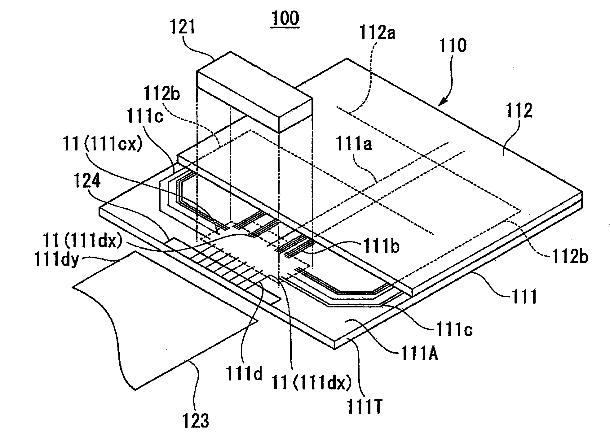
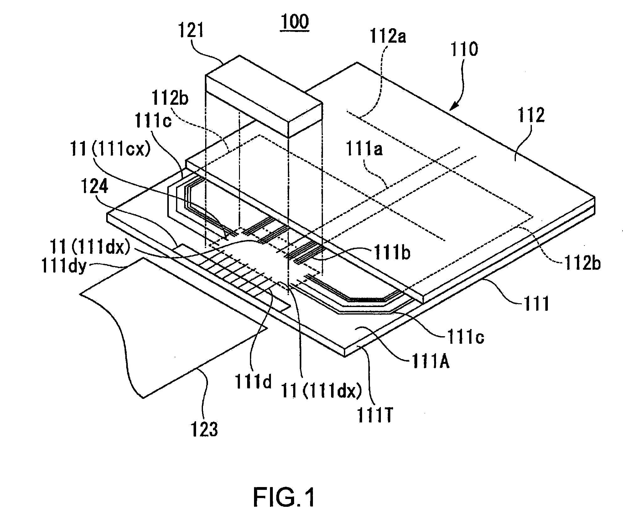
[0037]FIG. 1 is a schematic view showing a liquid crystal display to which an electronic component mounting structure according to a first embodiment of the invention is applied. First, an application example of the electronic component mounting structure according to this embodiment will be described with reference to FIG. 1.
[0038]In FIG. 1, a liquid crystal display 100 includes a liquid crystal panel 110 and an electronic component (liquid crystal-driving IC chip) 121. Note that the liquid crystal display 100 is provided with ancillary members (not shown), such as a polarizing plate, a reflection sheet, and a backlight, as necessary.
[0039]The liquid crystal panel 110 includes substrates 111 and 112 made of glass or synthetic resin. The substrate 111 and substrate 112 are disposed as opposed to each other, and bonded together using a sealing material (not shown). Liquid crystal (not shown), which is an electrooptic material, is sealed between the substrate 111 and substrate 112. El...
second embodiment
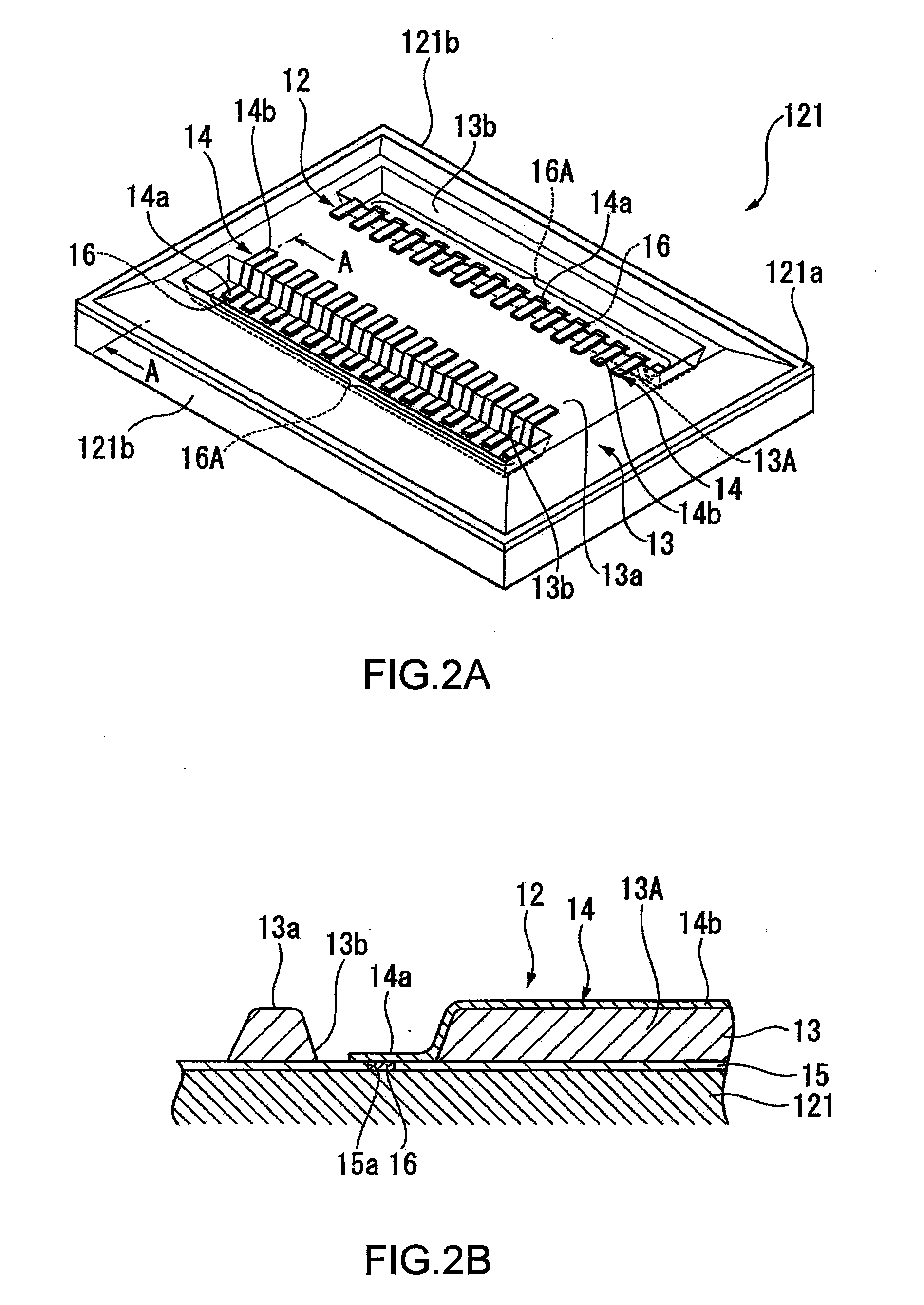
[0077]Hereafter, a second embodiment of the invention will be described. FIG. 5A is a plan view of an active face 131a of an electronic component 131 according to the second embodiment. FIG. 5B is a sectional view as seen in the direction of arrows D-D of FIG. 5A.
[0078]In the electronic component 131 according to this embodiment, two openings 13b and two openings 13c (second openings), that is, a total of four openings are made on the base resin 13. Specifically, in addition to the openings 13b made for the terminal lines 16A, the openings 13c that are located inside the openings 13b and extend in parallel with the openings 13b are made. The openings 13c have approximately the same size as that of the openings 13b and each take the shape of a rectangle in a plan view. Each opening 13c is made near the corresponding opening 13b at a predetermined distance from the opening 13b.
[0079]As in the above-mentioned embodiment, the multiple electrode terminals 16 are disposed in each opening...
third embodiment
[0084]Next, a third embodiment of the invention will be described. FIG. 6 is a plan view of an active face 141a of an electronic component 141 according to the third embodiment.
[0085]In the electronic component 141 according to this embodiment, one opening 13d is made on the base resin 13 in the form of a frame along the four sides of the electronic component 141. The opening 13d is commonly used by the all the electrode terminals 16 provided on the active face 141a, and all the electrode terminals 16 provided on the active face 141a are disposed inside the opening 13d. These electrode terminals 16 are disposed along the circumference direction of the opening 13d, and multiple electrode terminals 16 are disposed along each side of the electronic component 141. The portion of the base resin 13 surrounded by the opening 13d forms a protruding line portion, a cross section of which takes the shape of a rough trapezoid.
[0086]The conductive films 14 are provided in such a manner that the...
PUM
 Abstract
Description
Claims
Application Information