Environmental die seal enhancement for wafer level chip scale packages

a technology of scale package and environment die, which is applied in the direction of semiconductor devices, semiconductor/solid-state device details, electrical devices, etc., can solve the problems of limiting the leverage action of stress forces and the length of cracks, and achieve the effect of enhancing the strength and barrier properties of scribe seals, preventing damage during the assembly process, and minimizing the penetration of moisture in the dielectric layer of the di

Active Publication Date: 2010-04-01
TEXAS INSTR INC
View PDF8 Cites 93 Cited by
  • Summary
  • Abstract
  • Description
  • Claims
  • Application Information

AI Technical Summary

Benefits of technology

[0008]These and other problems associated with the prior art are addressed by the present invention, which provides a semiconductor device for use in a wafer level chip scale package (WLCSP), and a method for fabricating a semiconductor device for wafer level chip scale packaging. By providing redundant scribe seals, an inner scribe seal formed around a functional circuit area that does not extend all the way into the corners of the rectangular die, and an outer scribe seal following the perimeter of the die and into the corners, with the outer scribe seal having a continuous barrier wall towards the die edges, moisture penetration in dielectric layers of the die is minimized, and cracks and delamination are stopped near the die edges. Limiting the extent of the insulating layer or layers in the WLCSP to the functional circuit area also reduces the stresses caused by these layers near the die corners. Additional optional features are also provided to further enhance the strength and barrier properties of the scribe seals and the layers near the die corners, to terminate cracks and delamination at various levels within the dielectric stack of the die and the die protective overcoat, and to prevent damage during the WLCSP assembly process.

Problems solved by technology

This limits the length of the cracks, and hence limits the leverage action of the stress forces before they encounter a metal wall.

Method used


Image

  • Environmental die seal enhancement for wafer level chip scale packages
  • Environmental die seal enhancement for wafer level chip scale packages
  • Environmental die seal enhancement for wafer level chip scale packages

Examples


Embodiment Construction

[0019]While the making and using of various embodiments of the present invention are discussed in detail below, it should be appreciated that the present invention provides many applicable inventive concepts that can be embodied in a wide variety of specific contexts. The specific embodiments discussed herein are merely illustrative of specific ways to make and use the invention and do not delimit the scope of the invention.

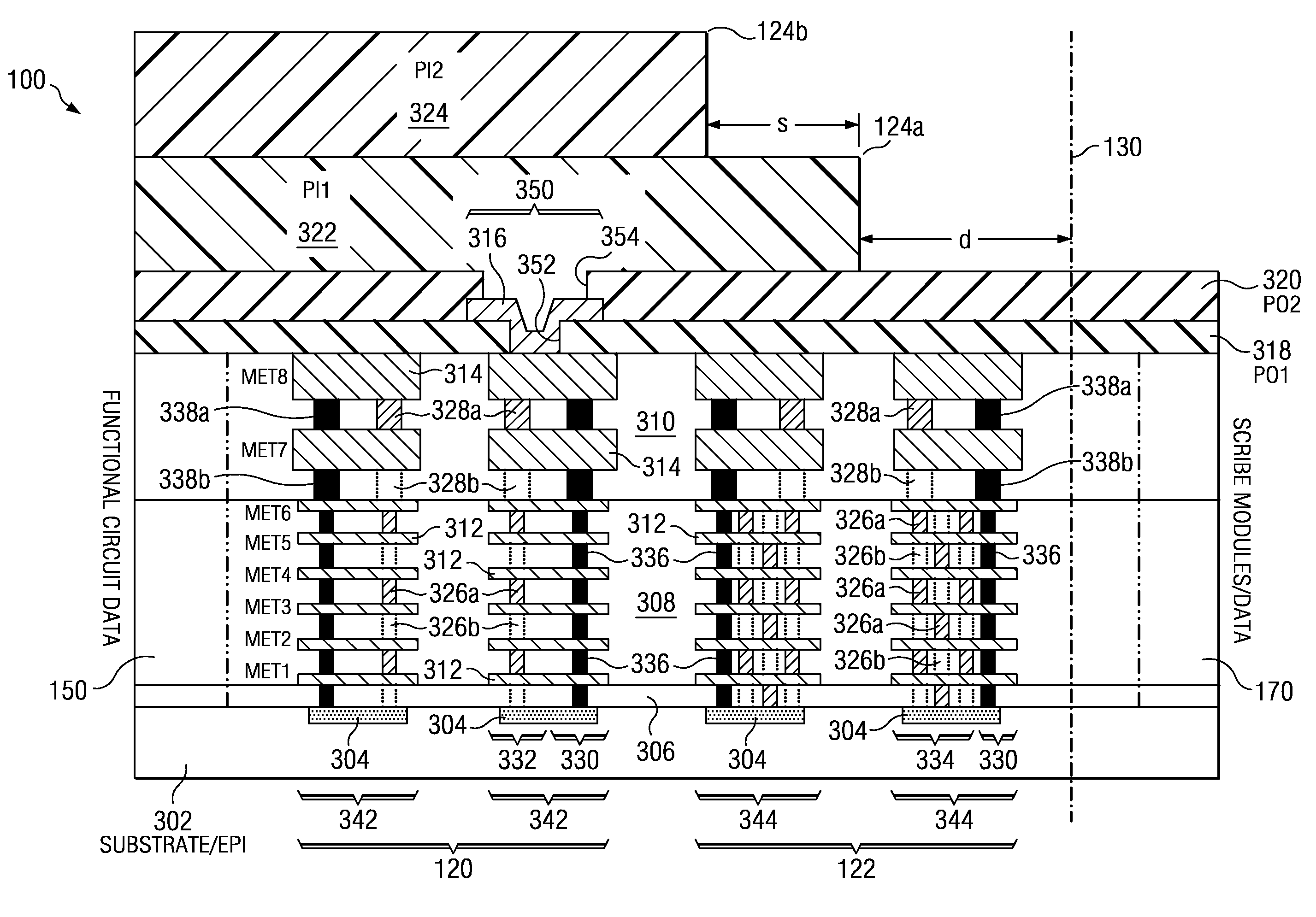
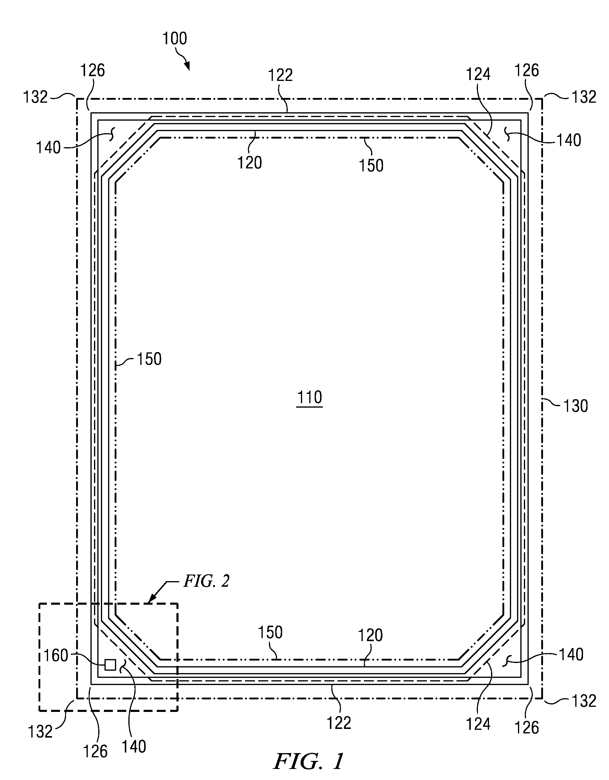
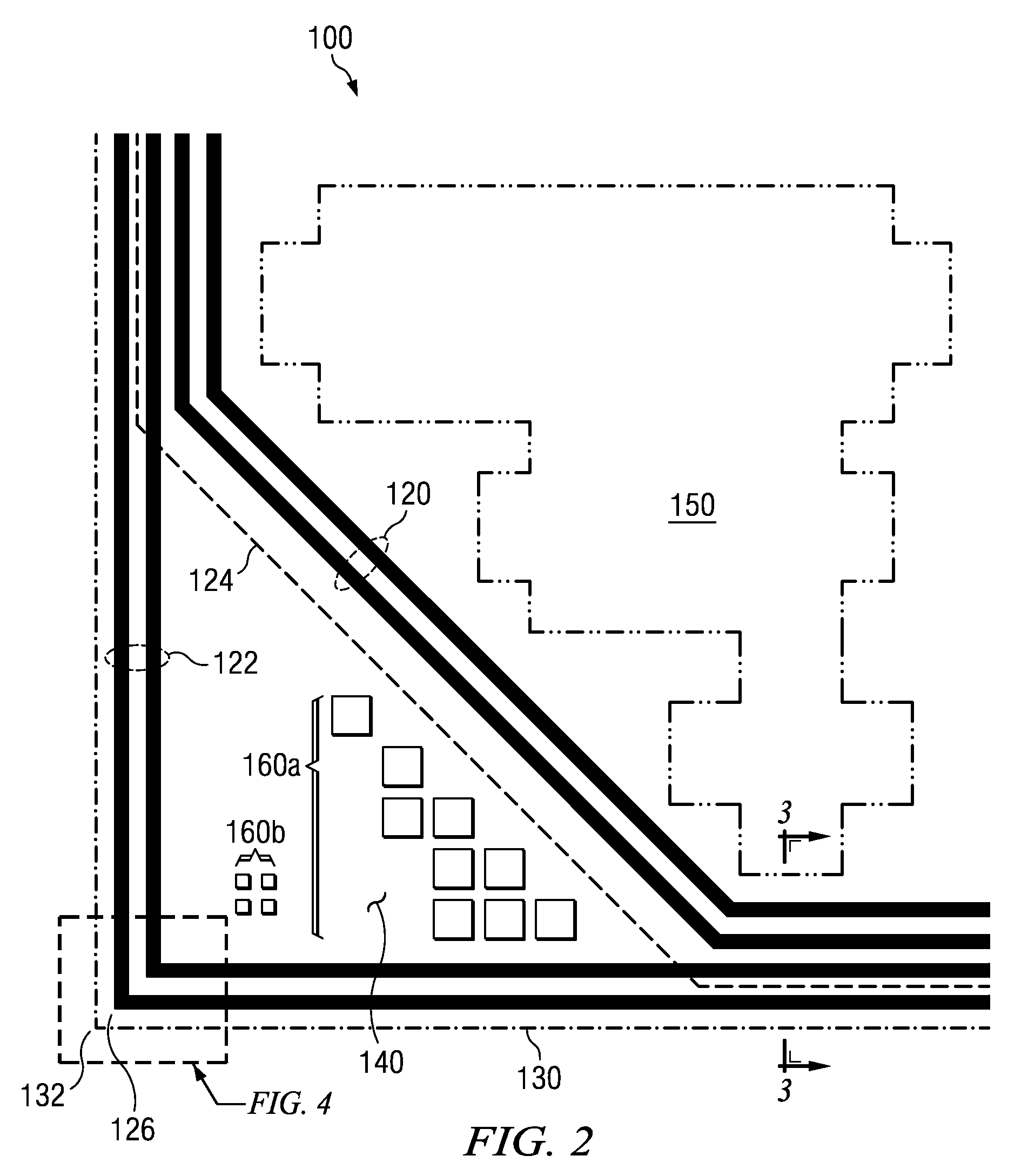
[0020]Referring now to FIG. 1, a simplified and schematic top view of a semiconductor device 100 according to the present invention is shown. The semiconductor device 100 includes a die 110, typically having a rectangular shape with four physical edges 130 created by a singulation process (sawing or scribing, typically sawing with a high-speed diamond wheel) and four physical corners 132. Functional circuit structures including active semiconductor devices and interconnects are confined to an area defined by perimeter 150. This perimeter may be diagonally removed...


PUM


Abstract

In a semiconductor device for use in a wafer level chip scale package (WLCSP) and a method for fabrication, an inner scribe seal is formed around a functional circuit area that does not extend all the way into the corners of the rectangular die, and an outer scribe seal follows the perimeter of the die and into the corners, with the outer scribe seal having a continuous barrier wall towards the die edges so that moisture penetration in dielectric layers of the die is minimized, and cracks and delamination are stopped near the die edges. Limiting the extent of the insulating layer or layers in the WLCSP to cover the functional circuit area also reduces the stresses caused by these layers near the die corners. Other features further enhance the strength and barrier properties of the scribe seals and the layers near the die corners, terminate cracks and delamination at various levels within the dielectric stack of the die and the die protective overcoat, and prevent damage during the WLCSP assembly process.

Description

CROSS-REFERENCE TO RELATED APPLICATIONS[0001]This application claims the benefit of U.S. Provisional Application No. 61 / 099,357, filed Sep. 23, 2008 by Jeffrey Alan West, the entire contents of which are hereby incorporated by reference.BACKGROUND OF THE INVENTION[0002]1. Field of the Invention[0003]The present invention is related in general to the field of semiconductor device assembly and packaging, and more specifically to fabricating integrated circuit (IC) devices that are protected against potential damage caused by moisture, contamination, and stress induced defects such as cracks and delamination when incorporated into wafer level chip scale packages.[0004]2. Description of the Related Art[0005]It is well known to use a scribe seal (which may also be referred to as a die seal, an edge seal, or a seal ring) to protect a die against potential damage caused by stress induced defects such as crack formation and delamination formed during processes such as sawing, wirebonding or...

Claims


Application Information

Patent Timeline
Patent Type & Authority Applications(United States)
IPC IPC(8): H01L23/544H01L21/302
CPCH01L23/3114H01L23/562H01L23/564H01L23/585H01L2924/0002H01L2924/00
Inventor WEST, JEFFREY A.BEDDINGFIELD, STANLEY CRAIG
Owner TEXAS INSTR INC
Why Eureka
Try Eureka