Plasma display panel and method of manufacturing the same and plasma display device using the plasma display panel

a technology of plasma display panel and plasma display panel, which is applied in the manufacture of electric discharge tubes/lamps, electrode systems, instruments, etc., can solve the problems of new important issues such as the improvement of discharge delay, and achieve the effects of reducing the display period, preventing display errors, and reducing the delay

Inactive Publication Date: 2010-04-01
MAXELL HLDG LTD
View PDF6 Cites 3 Cited by
  • Summary
  • Abstract
  • Description
  • Claims
  • Application Information

AI Technical Summary

Benefits of technology

[0011]If these discharge delays are long, an address time has to be extended to prevent display errors, and it leads to adverse effects such as shortened display period relating to image formation. Therefore, the discharge delay is preferred to be shortened for the PDP.
[0012]In a gas discharge, charged particles in a space (discharge space) are accelerated by an external electric field and bombarded against other gas molecules, so that the gas molecules are ionized to increase the number of ionized particles. Meanwhile, a discharge is not started unless charged particles are supplied at first, and the discharge start is delayed until charged particles are supplied. Therefore, as supplying more priming electrons (initial charged particles) to be pilot light (priming) of a discharge in the discharge space, the discharge delay is further shortened.

Problems solved by technology

As a result, improvement of a discharge delay has been a new important issue.

Method used


Image

  • Plasma display panel and method of manufacturing the same and plasma display device using the plasma display panel
  • Plasma display panel and method of manufacturing the same and plasma display device using the plasma display panel
  • Plasma display panel and method of manufacturing the same and plasma display device using the plasma display panel

Examples


Embodiment Construction

[0044]Before describing the invention of the present application in detail, meanings of terms in the present application will be explained as follows.

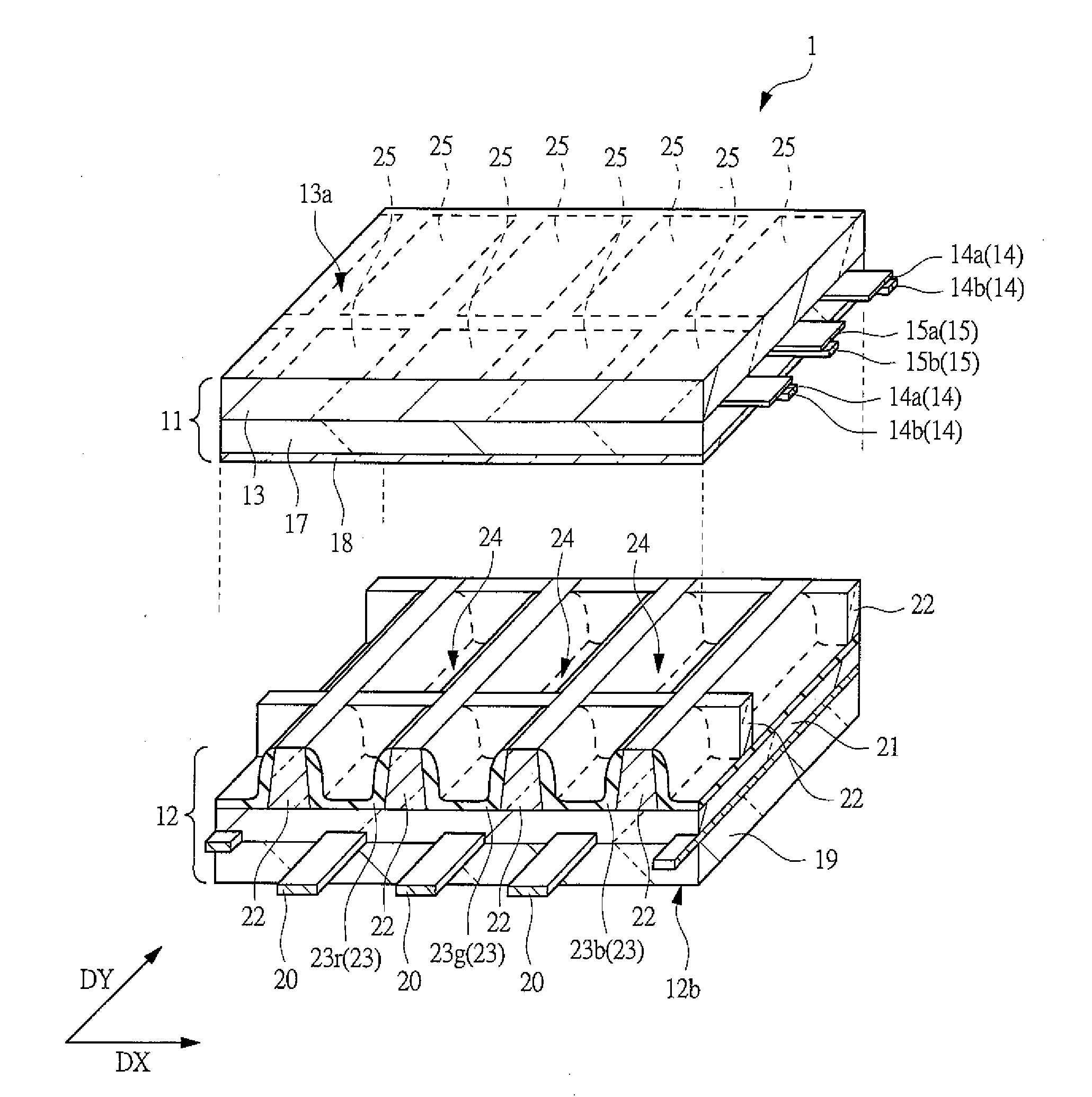
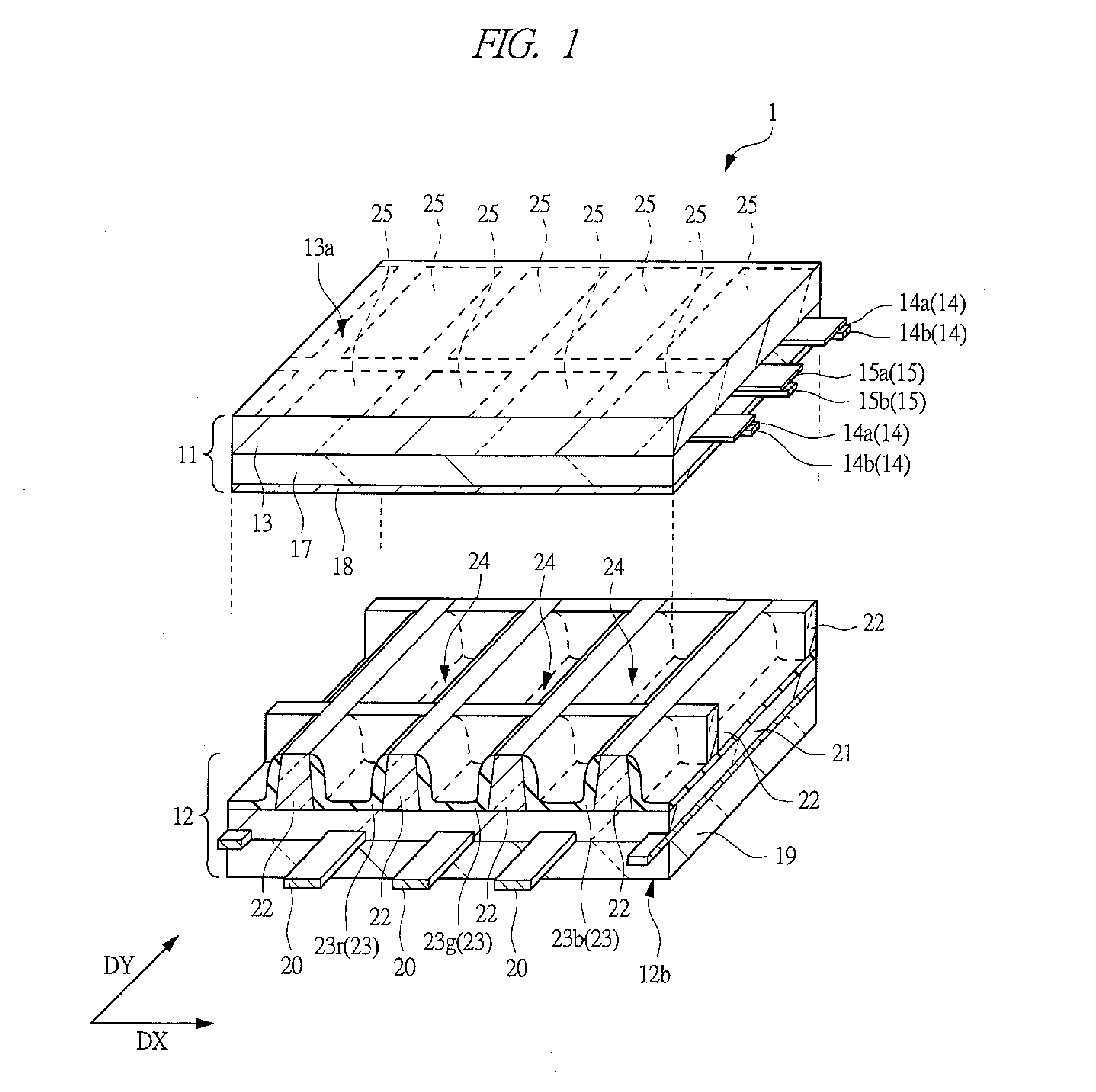
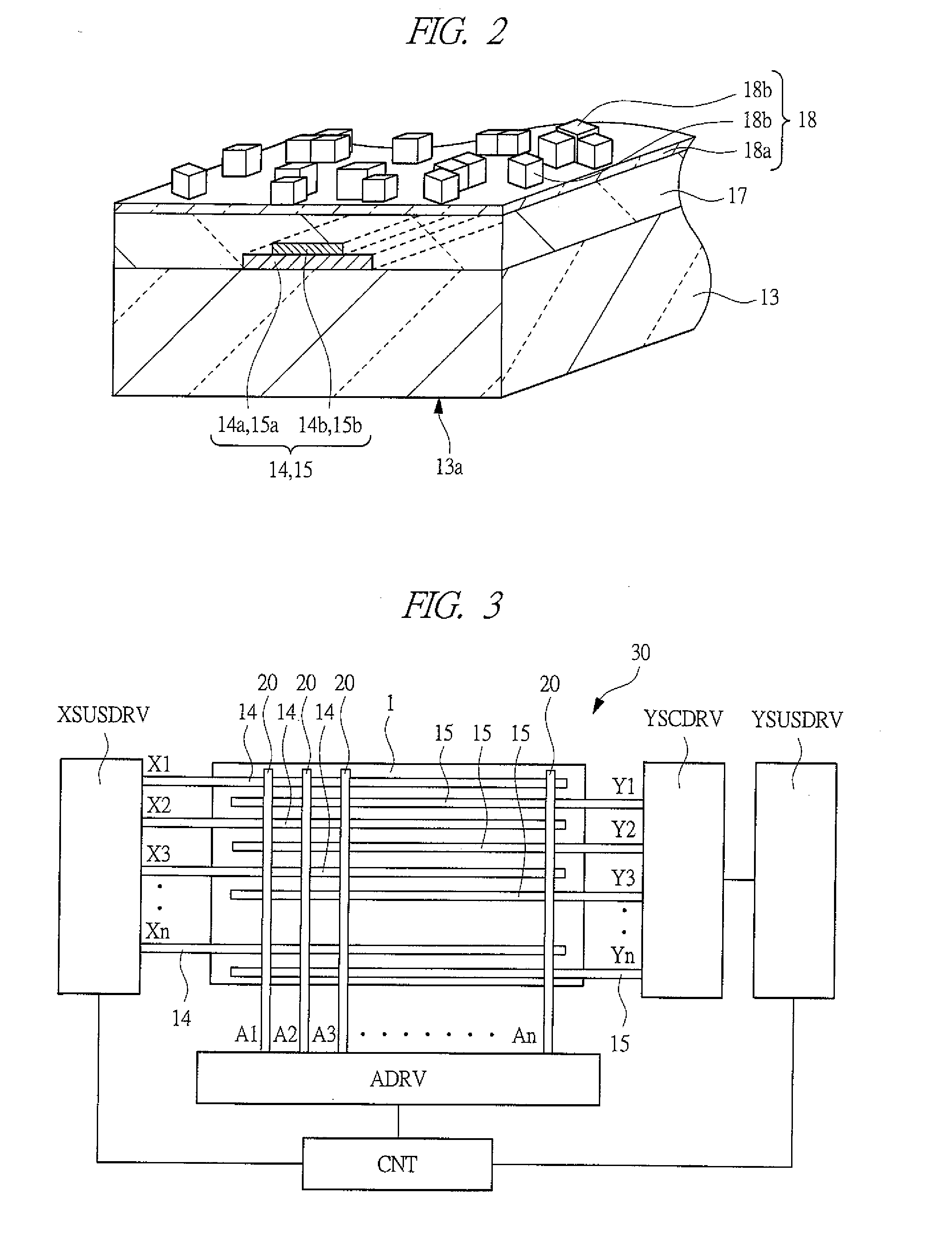
[0045]A plasma display panel (PDP) is a display panel having a substantially plane plate shape in which gas discharge is generated within a discharge cell formed between paired plates which are oppositely arranged to excite phosphors by excitation light generated in the gas discharge, so that a desired image is formed. There are various configuration examples in an internal structure and a component material of the PDP depending on required performance or a driving method. However, all of these configuration examples are included except a configuration example which cannot be apparently employed in principle.

[0046]A plasma display module (PDP module) is a module having: a PDP; a chassis member which is arranged on opposite side of a display surface of the PDP for supporting the PDP; and a circuit board which is arranged on a back surfa...


PUM


Abstract

Increase of an address voltage change amount of a PDP is suppressed. X and Y electrodes which are a display electrode pair arranged on a plate; a dielectric layer covering the X and Y electrodes; and a protective layer covering the dielectric layer are provided. The protective layer includes an MgO film deposited on a surface of the dielectric layer and a plurality of MgO crystalline particles attached on the MgO film. Also, by using (110) orientation as a crystal orientation of the MgO film, a crystal density of the MgO film can be increased, so that an increase of the address voltage change amount can be suppressed.

Description

CROSS-REFERENCE TO RELATED APPLICATION[0001]The present application claims priority from Japanese Patent Application No. JP 2008-248119 filed on Sep. 26, 2008, the content of which is hereby incorporated by reference into this application.BACKGROUND OF THE INVENTION[0002]The present invention relates to a plasma display panel and a method of manufacturing the same. More particularly, the present invention relates to a technique effectively applied to a plasma display panel in which a plurality of MgO crystalline particles are attached on a surface of a protective film.[0003]Plasma display panel (PDP) is a display panel which displays images by generating gas discharge in a discharge space called a cell in which a discharge gas such as rare gas is filled to excite a phosphor by vacuum ultraviolet rays generated by the gas discharge.[0004]Currently, generally commercialized PDPs employing an AC (alternate current) driving method are surface discharge type. In the surface discharge typ...

Claims


Application Information

Patent Timeline
Patent Type & Authority Applications(United States)
IPC IPC(8): G09G5/00H01J17/49H01J9/00H01J9/02H01J11/12H01J11/22H01J11/24H01J11/26H01J11/34H01J11/40
CPCH01J11/40H01J11/12
Inventor KAWASAKI, TATSUHIKOWADA, MASAYUKIOHTOMI, ATSUO
Owner MAXELL HLDG LTD
Why Eureka
Try Eureka