Mask pattern forming method, fine pattern forming method, and film deposition apparatus

a technology of mask pattern and forming method, which is applied in the direction of photomechanical equipment, instruments, photosensitive material processing, etc., can solve the problems of increasing manufacturing costs, dust or foreign matter adhesion to the surface of resist patterns, and devices that require fine patterns. to achieve the effect of reducing the cost of the forming process

Active Publication Date: 2010-04-01
TOKYO ELECTRON LTD
View PDF3 Cites 355 Cited by
  • Summary
  • Abstract
  • Description
  • Claims
  • Application Information

AI Technical Summary

Benefits of technology

[0018]In an aspect of this disclosure, there are provided a mask pattern forming method, a fine pattern forming method and a film deposition apparatus which are capable of reducing the cost of the process of forming a mask pattern (or fine pattern) from an oxide film formed on a pattern organic film.

Problems solved by technology

However, the microstructures of the latest semiconductor devices have come to require a pitch of fine patterns which is below a resolution limit of the photolithographic technique.
However, in the above-described fine pattern forming method in which the film deposition process to form the silicon oxide on the pattern organic film is combined with the fine patterns formed by SWT or LLE, the following problems will arise.
This will increase the manufacturing cost.
However, if the wafer is taken out from the ashing device after the slimming process is finished, dust or foreign matter will adhere to the surface of the resist pattern.
Moreover, when the slimming process or the film deposition process is performed, it is difficult to maintain the dimensions of resist patterns in order to make the difference between a top width and a bottom width of each resist pattern small.
For this reason, it is difficult to form fine patterns with a good configuration.

Method used


Image

  • Mask pattern forming method, fine pattern forming method, and film deposition apparatus
  • Mask pattern forming method, fine pattern forming method, and film deposition apparatus
  • Mask pattern forming method, fine pattern forming method, and film deposition apparatus

Examples


example 1

(A) Slimming Process in Film Deposition Apparatus

Oxygen-containing gas: O2 gas

[0169]Substrate temperature: no heating

Internal pressure of film deposition apparatus: 66.7-227 Pa

Gas mass flow: 5-30 slm

RF generator frequency: 13.56 MHz

RF generator power: 50-500 W

(B) Film Deposition Process

(1) Source Gas Supplying Conditions

Source gas: DIPAS (LTO520)

[0170]Substrate temperature: no heating

Internal pressure of film deposition apparatus: 26.7-667 Pa

Gas mass flow: 50-1000 sccm

Supplying time: 1-10 sec

(2) Oxidizing Gas Supplying Conditions

[0171]Oxidizing gas: oxygen gas

Substrate temperature: no heating

Internal pressure of film deposition apparatus: 66.7-227 Pa

Gas mass flow: 5-30 slm

Supplying time: 5-30 sec

RF generator frequency: 13.56 MHz

RF generator power: 50-500 W

(3) Repetition Conditions

[0172]Total cycle: 140-150 cycles

[0173]FIGS. 9A and 9B illustrate SEM photographs (left-hand side) of the cross section of the resist pattern from the slanting upper part and the front part, respectively, a...

example 2

(1) Source Gas Supplying Conditions

Source gas: TMA

[0289]Substrate temperature: no heating

Internal pressure of film deposition apparatus: 39.9 Pa

Gas mass flow: 100 sccm

Supplying time: 5 sec

(2) Oxidizing Gas Supplying Conditions

[0290]Oxidizing gas: ozone gas+oxygen gas

Substrate temperature: no heating

Internal pressure of film deposition apparatus: 133 Pa

Ozone gas flow rate: 200 g / m3

Oxygen gas mass flow: 10.0 slm

Supplying time: 15 sec

(3) Repetition Conditions

[0291]Sum cycle: 210 cycles

example 5

(A) Film Deposition Conditions of Aluminum Oxide Film

[0366](1) Source gas supplying conditions

Source gas: TMA

[0367]Substrate temperature: no heating

Internal pressure of film deposition apparatus: 39.9 Pa

Gas mass flow: 100 sccm

Supplying time: 5 sec

(2) Oxidizing gas supplying conditions

Oxidizing gas: ozone gas+oxygen gas

Substrate temperature: no heating

Internal pressure of film deposition apparatus: 133 Pa

Ozone gas flow rate: 200 g / m3

Oxygen gas mass flow: 10.0 slm

Supplying time: 15 sec

(3) Repetition conditions

Total cycle: 35 cycles

(B) Film Deposition Conditions of Silicon Oxide Film

[0368](1) Source gas supplying conditions

Source gas: DIPAS (LTO520)

[0369]Substrate temperature: no heating

Internal pressure of film deposition apparatus: 26.7-667 Pa

Gas mass flow: 50-1000 sccm

Supplying time: 1-10 sec

(2) Oxidizing gas supplying conditions

Oxidizing gas: oxygen gas

Substrate temperature: no heating

Internal pressure of film deposition apparatus: 66.7-227 Pa

Gas mass flow: 5-30 slm

Supplying time: ...


PUM

PropertyMeasurementUnit
thicknessaaaaaaaaaa
thicknessaaaaaaaaaa
thicknessaaaaaaaaaa

Abstract

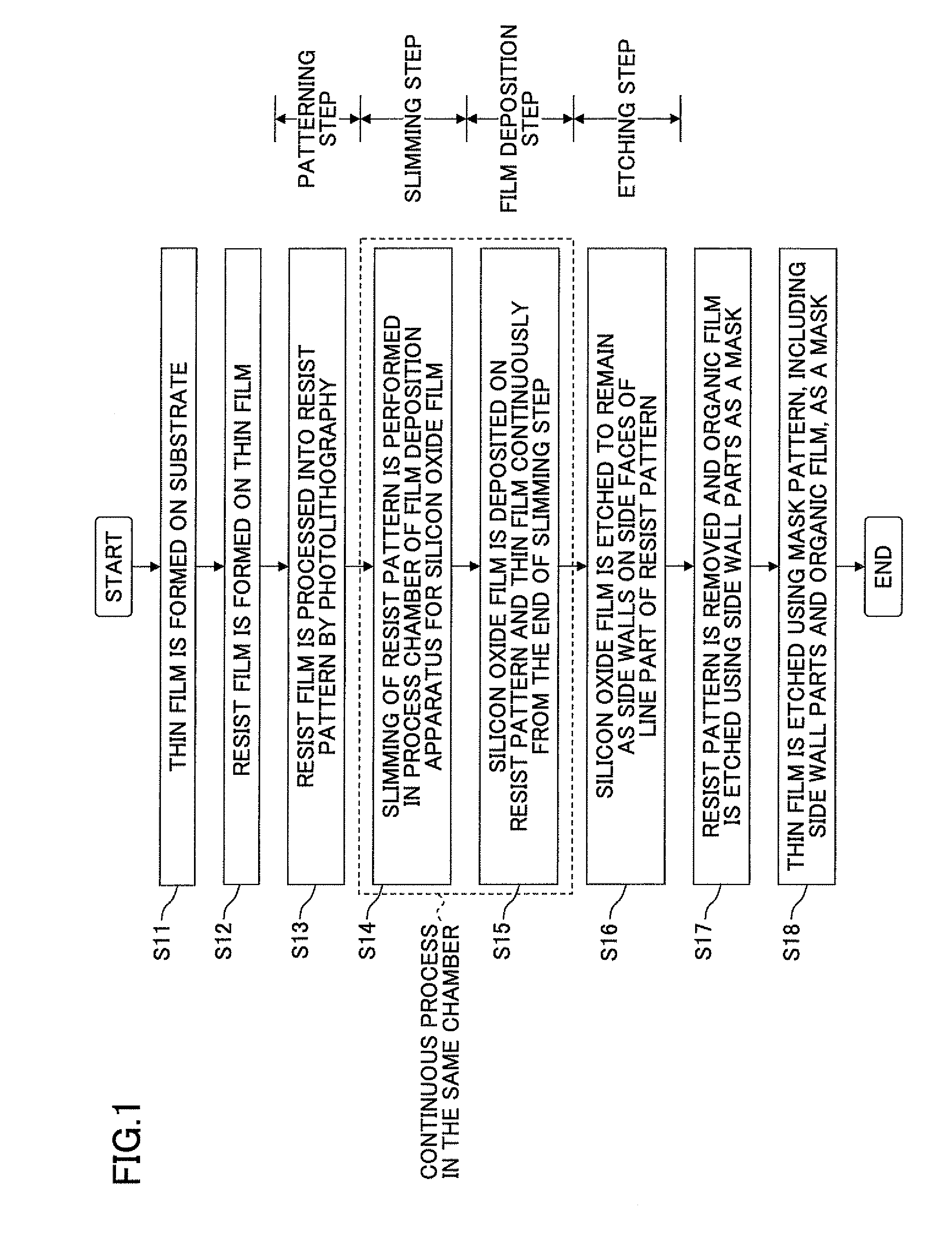
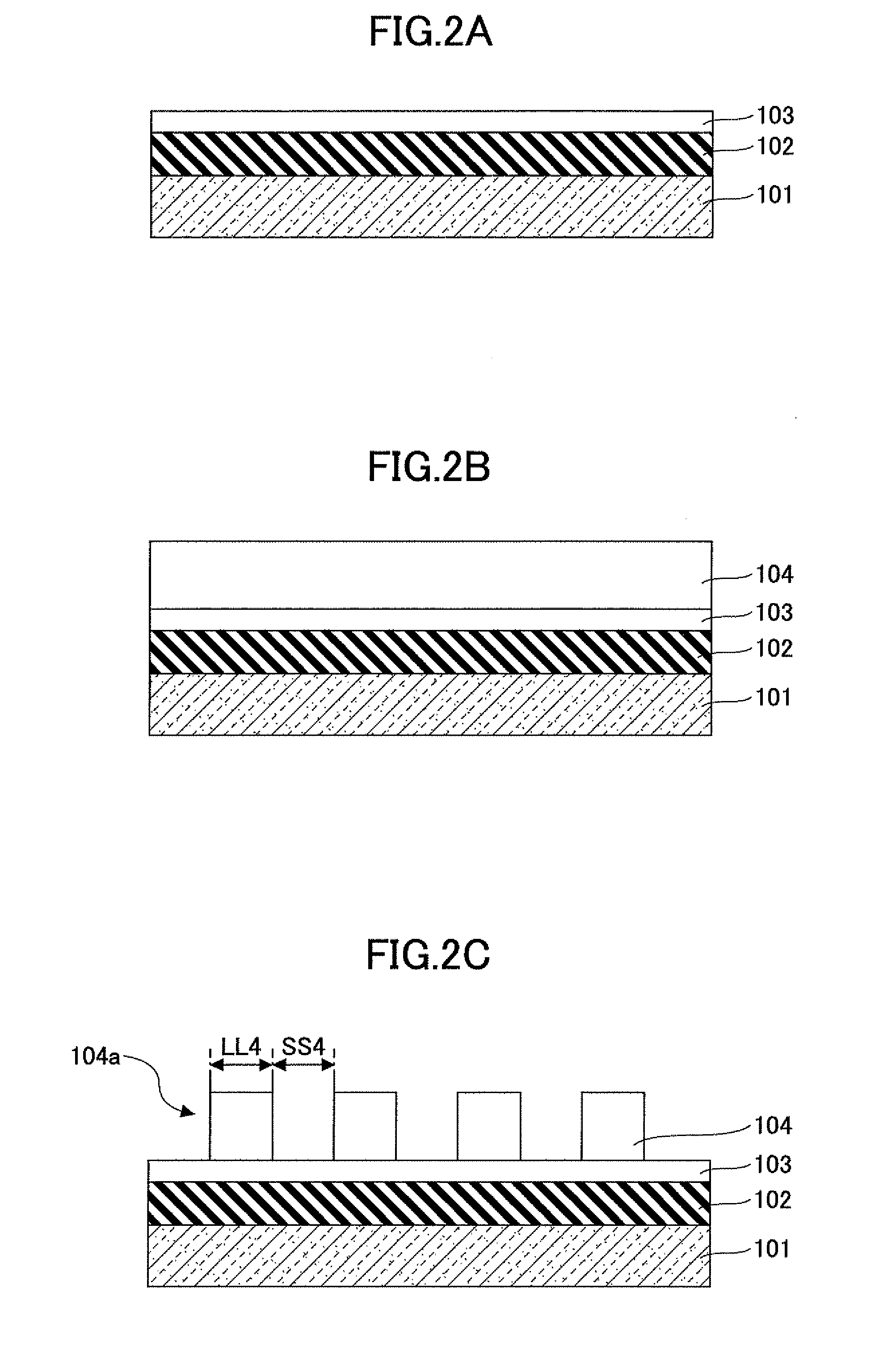
In a mask pattern forming method, a resist film is formed over a thin film, the resist film is processed into resist patterns having a predetermined pitch by photolithography, slimming of the resist patterns is performed, and an oxide film is formed on the thin film and the resist patterns after an end of the slimming step in a film deposition apparatus by supplying a source gas and an oxygen radical or an oxygen-containing gas. In the mask pattern forming method, the slimming and the oxide film forming are continuously performed in the film deposition apparatus.

Description

CROSS-REFERENCE TO RELATED APPLICATION[0001]This application is based upon and claims the benefit of priority of Japanese patent application No. 2008-251679, filed on Sep. 29, 2008, and Japanese patent application No. 2009-206443, filed on Sep. 7, 2009, the contents of which are incorporated herein by reference in their entirety.BACKGROUND OF THE INVENTION[0002]1. Field of the Invention[0003]This invention relates to a mask pattern forming method, a fine pattern forming method and a film deposition apparatus which are used for semiconductor processes. More particularly, the invention relates to a mask pattern forming method, a fine pattern forming method and a film deposition apparatus which are capable of improving the precision to correct the pattern dimensions when forming patterns at pitches smaller than a resolution limit of an exposure device, without increasing the manufacturing cost.[0004]2. Description of the Related Art[0005]With high integration of semiconductor devices, ...

Claims


Application Information

Patent Timeline
Patent Type & Authority Applications(United States)
IPC IPC(8): G03F7/20H01L21/46
CPCC23C16/02H01L21/027C23C16/403C23C16/45536G03F7/40H01L21/02164H01L21/02178H01L21/02219H01L21/0228H01L21/0337H01L21/0338H01L21/31138H01L21/31144H01L21/31608H01L21/31616H01L21/32139H01L21/76816C23C16/402H01L21/2053H01L21/0276H01L21/0274H01J37/32091H01J37/32834H01J37/3244H01L21/02274
Inventor HASEBE, KAZUHIDENAKAJIMA, SHIGERUOGAWA, JUNMURAKAMI, HIROKI
Owner TOKYO ELECTRON LTD
Why Eureka
Try Eureka