
Method for detecting memory training result and computer system using such method

a memory training and computer system technology, applied in the field of methods, can solve problems such as possible problems, data not being accurately read out or written into the dram chip, and possible propagation delays of all signals

Inactive Publication Date: 2010-04-01
ASUSTEK COMPUTER INC
View PDF9 Cites 18 Cited by
  • Summary
  • Abstract
  • Description
  • Claims
  • Application Information

AI Technical Summary

Problems solved by technology

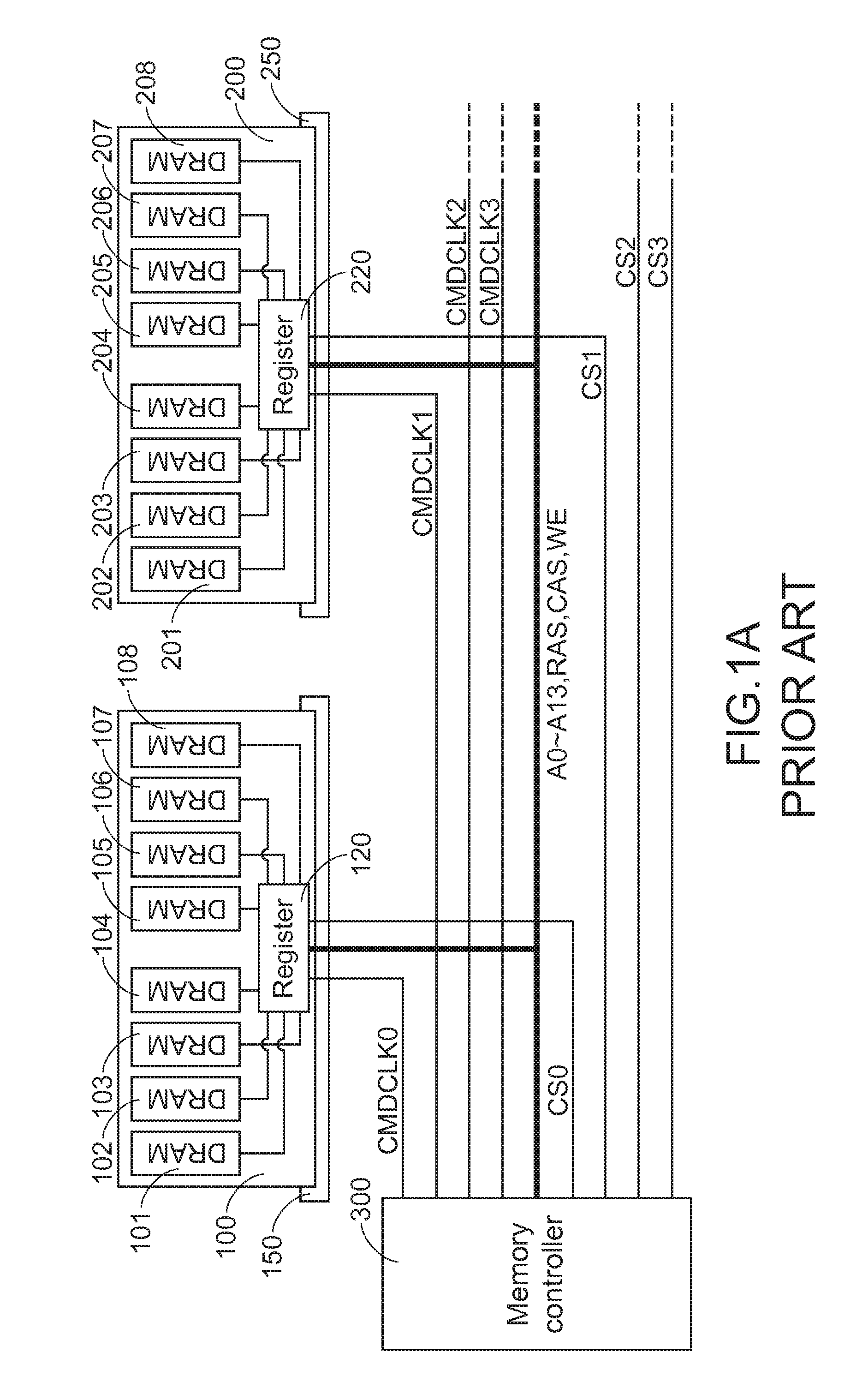
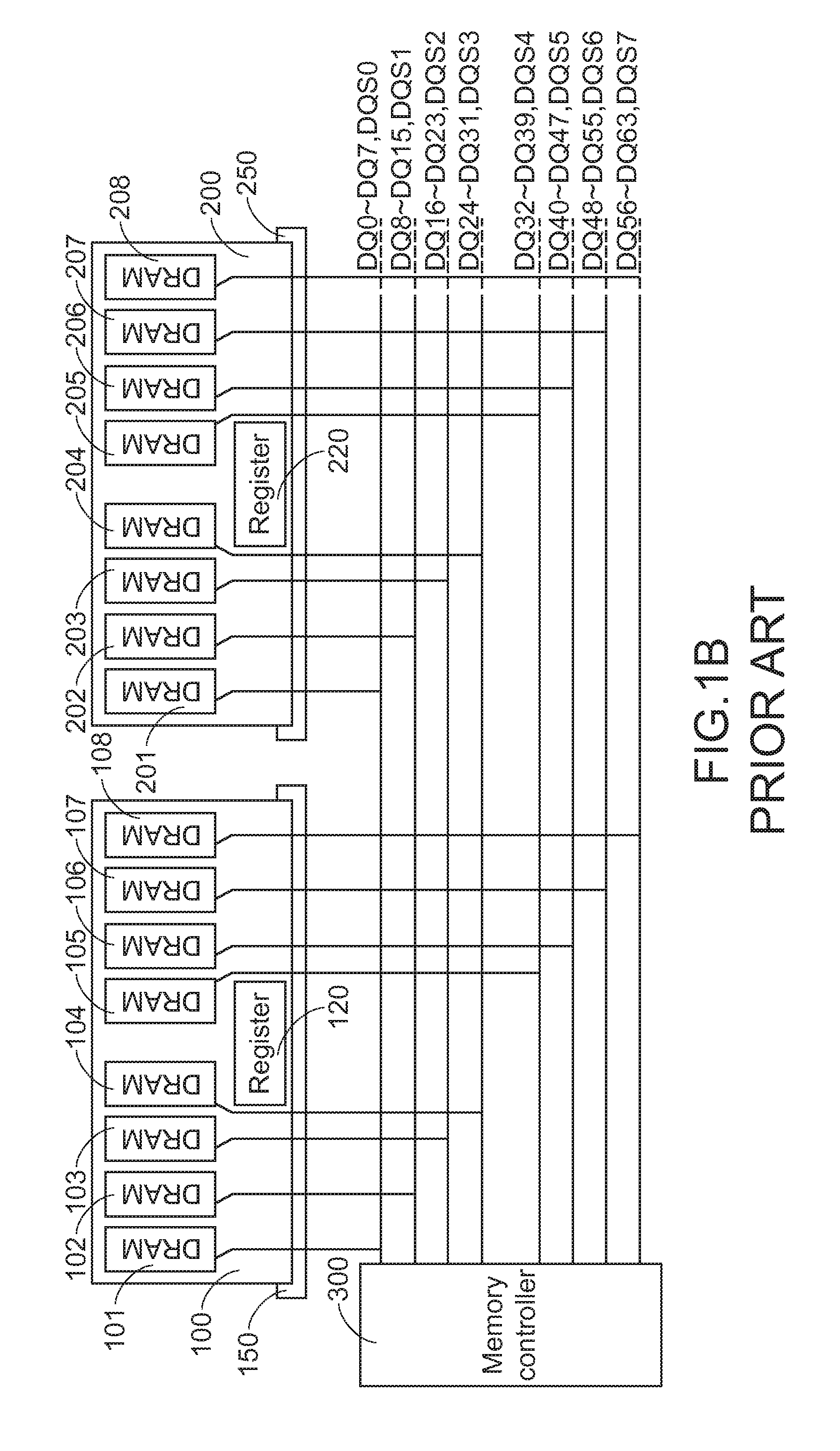
If the memory modules available from different manufacturers are plugged into the memory module insertion slots of the same motherboard of a computer system, some problems are possibly incurred.
For example, if the DRAM chips and / or the layout configurations of the daughter boards of different memory modules are very distinguished, the propagation delays of all signals are not consistent.
Under this circumstance, the data fail to be accurately read out or written into the DRAM chips.
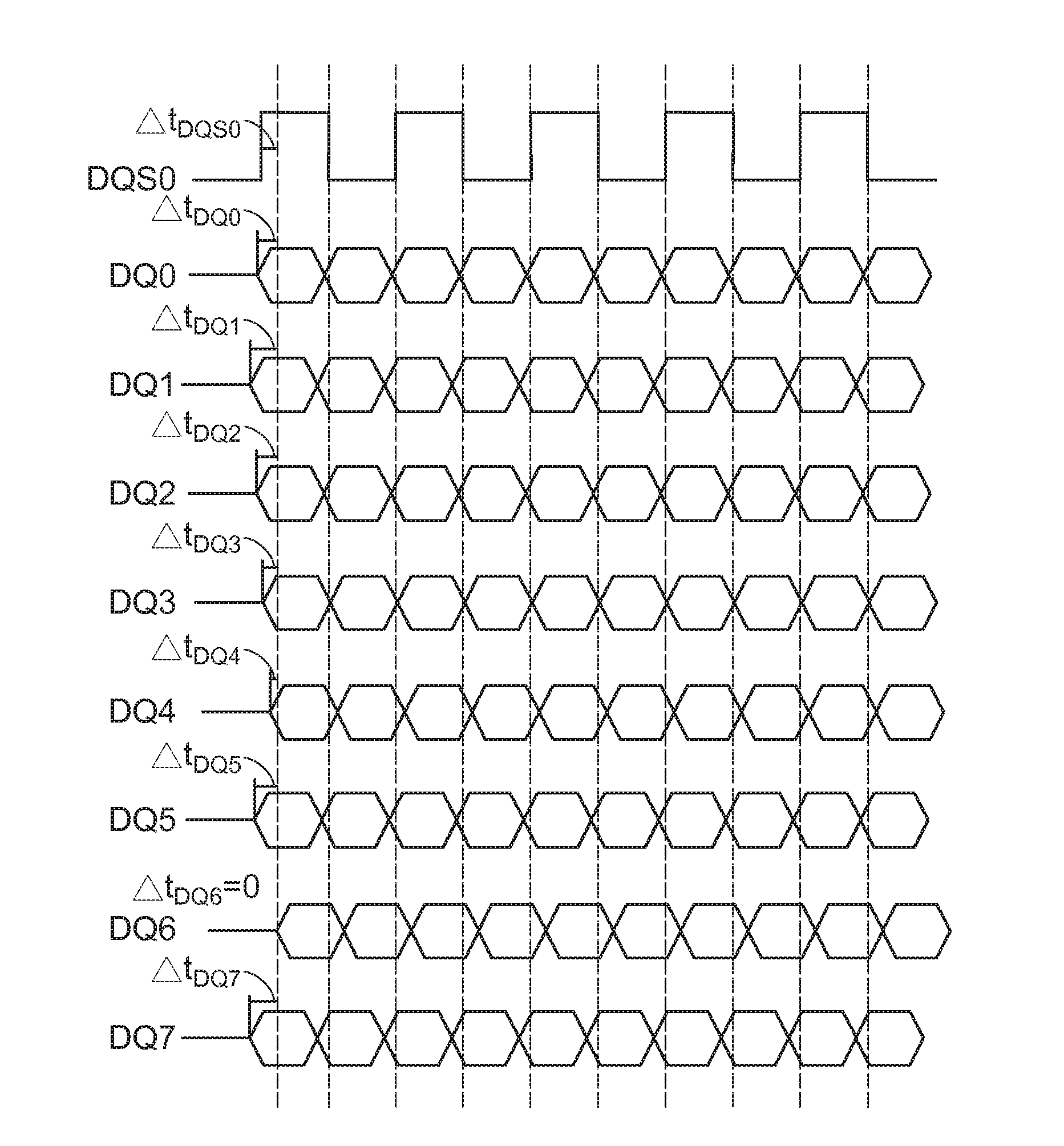
As a consequence, the data of the DQ6 signal may fail to be accurately read out or written into the DRAM chips.
Under this circumstance, the operations of the memory modules are abnormal.
Due to the difference between the daughter boards of supporting different memory modules, the difference between the DRAM chips and the speed difference, some memory modules fail to be successfully read out or written in.
Since the DQ6 signal and the DQS0 signal are not aligned with each other, the memory controller or the DRAM chips fail to accurately read out the data of the DQ6 signal.
As the types of memory modules are more and more diverse, the processes for testing and troubleshooting the memory modules become very troublesome and inefficient.
Under this circumstance, the delivery time of the motherboard from the factory is usually delayed.

Method used


Image

  • Method for detecting memory training result and computer system using such method
  • Method for detecting memory training result and computer system using such method
  • Method for detecting memory training result and computer system using such method

Examples


first embodiment

[0040]FIG. 4A is a schematic functional block diagram illustrating a computer system for recording the memory training result according to the present invention. As shown in FIG. 4A, the computer system comprises a central processing unit (CPU) 500, a chipset 505, a BIOS 508, a non-volatile memory 506 (e.g. a flash memory), and a memory device 510. The chipset 505 includes a north bridge chip 502 and a south bridge chip 504. The north bridge chip 502 is connected to the memory device 510, the CPU 500 and the south bridge chip 504. The south bridge chip 504 is connected to the north bridge chip 502, the BIOS 508 and the non-volatile memory 506. The memory device 510 includes at least one memory module (not shown). The BIOS 508 includes a memory training program 509. In addition, a memory controller 503 is integrated into the north bridge chip 502 of the chipset 505.

second embodiment

[0041]FIG. 4B is a schematic functional block diagram illustrating a computer system for recording the memory training result according to the present invention. As shown in FIG. 4B, the computer system comprises a central processing unit (CPU) 550, a chipset 555, a BIOS 558, a non-volatile memory 556 and a memory device 560. The chipset 555 includes a north bridge chip 552 and a south bridge chip 554. The CPU 550 is connected to the memory device 560. The north bridge chip 552 is connected to the CPU 550 and the south bridge chip 554. The south bridge chip 554 is connected to the north bridge chip 552, the BIOS 558 and the non-volatile memory 556. The memory device 560 includes at least one memory module (not shown). The BIOS 558 includes a memory training program 559. In addition, a memory controller 551 is integrated into the CPU 550.

[0042]Please refer to FIG. 4A again. During the booting of the computer system, when the memory training program 509 included in the BIOS 508 is exe...


PUM


Abstract

A method for detecting a memory training result includes the following steps. Firstly, a computer system is booted. Then, a memory training program included in a basic input output system of the computer system is executed, thereby obtaining a plurality of reading time parameters and a plurality of writing time parameters. Afterwards, the reading time parameters and the writing time parameters are recorded into a non-volatile memory. The computer system includes a central processing unit, a memory device, a chipset, a basic input output system, and a non-volatile memory. The memory device includes a memory module. The chipset is connected to the memory module and the central processing unit, and includes a memory controller. The basic input output system is connected to the chipset and includes a memory training program. The non-volatile memory is connected to the chipset.

Description

FIELD OF THE INVENTION[0001]The present invention relates to a method of detecting a memory training result, and more particularly to a method of detecting a memory training result in a computer system. The present invention also relates to a computer system using such a method.BACKGROUND OF THE INVENTION[0002]Generally, a memory controller is mounted on a motherboard of a computer system. The memory controller could be integrated into a north bridge chip or a central processing unit (CPU). A memory module such as a dual in-line memory module (DIMM) is usually plugged into a memory module insertion slot (e.g. a DIMM insertion slot) of the motherboard. As such, the memory controller and the memory module could exchange data with each other.[0003]Generally, the memory controller and the memory module insertion slot are soldered on the motherboard. In addition, the memory controller and the memory module insertion slot are electrically connected with each other via metallic traces of t...

Claims


Application Information

Patent Timeline
IPC IPC(8): G06F15/177G06F12/00
CPCG11C5/04G11C29/50G11C2029/4402G11C2029/0407G11C29/50012
Inventor LO, NAN-KUN
Owner ASUSTEK COMPUTER INC
Learn More